
A UWB Low Noise Monolithic Integrated Amplifier
A single-chip integrated, low-noise technology, applied in the direction of improving the amplifier to expand the bandwidth, improving the amplifier to reduce the impact of noise, etc., can solve the problems of reducing the service life of the battery, the working bandwidth cannot be satisfied, and the gain is reduced, so as to prolong the service life, Good broadband input and output matching, reducing the effect of parasitic inductance
Patent Information
- Authority / Receiving Office
- CN · China
- Patent Type
- Patents(China)
- Current Assignee / Owner
- Publication Date
- 2017-01-18
Smart Images
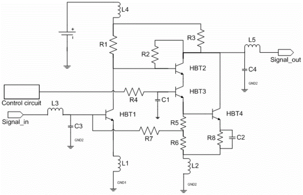
Figure 1
Abstract
Description
technical field
[0001] The invention relates to an integrated amplifier, in particular to an ultra-wideband low-noise monolithic integrated amplifier. Background technique
[0002] In the face of tight wireless communication resources, since the FCC (Federal Communications Commission of the United States) allocated the 3.1GHz-10.6GHz frequency band to ultra-wideband UWB (Ultra-Wide Band) and approved ultra-wideband UWB civilian use, wireless personal area network (WPAN) ), home network connection and short-range radar and other fields have achieved rapid development, and thus have broad market application prospects.
[0003] At present, there are two main methods of ultra-wideband communication. One is pulse ultra-wideband, which uses short-time impact pulses as information carriers, and carries information through PPM, PAM, etc. Modulation at the nanosecond level) to obtain very wide bandwidth; the other is multi-band ultra-wideband, which carries information through MB-OF...
Examples
Embodiment Construction
[0022] The present invention will be further described below in conjunction with accompanying drawing.
[0023] see figure 1 , an ultra-broadband low-noise monolithic integrated amplifier of the present invention includes a first-stage amplifying circuit and a second-stage amplifying circuit, the first-stage amplifying circuit includes a first transistor HBT1, and the second-stage amplifying circuit includes a second transistor HBT2 and the third transistor HBT3, the present invention also includes a third-stage amplifying circuit, the third-stage amplifying circuit includes a control current input terminal Control circuit, a fourth resistor R4, a first filter capacitor C1 and a fourth transistor HBT4.
[0024] The base of the first transistor HBT1 is connected to the signal input terminal, and the collector of the first transistor HBT1 is the signal output terminal of the first-stage amplifying circuit.
[0025] The collector of the first transistor HBT1 is connected with th...