
An injection-enhanced low-power injection-locked frequency tripler with wide locking range
An injection locking and injection enhancement technology, applied in power oscillators, electrical components, etc., can solve the problems of large power consumption, wide locking range, and increased injection tube size, and achieve low DC power consumption, wide locking range, and low power consumption. consumption effect
Patent Information
- Authority / Receiving Office
- CN · China
- Patent Type
- Patents(China)
- Current Assignee / Owner
- Publication Date
- 2017-05-10
- Estimated Expiration
- Not applicable · inactive patent
Smart Images
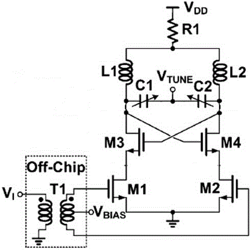
Figure 1 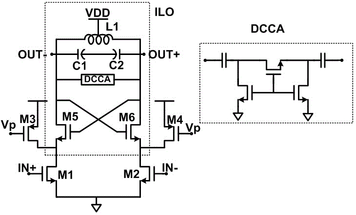
Figure 2 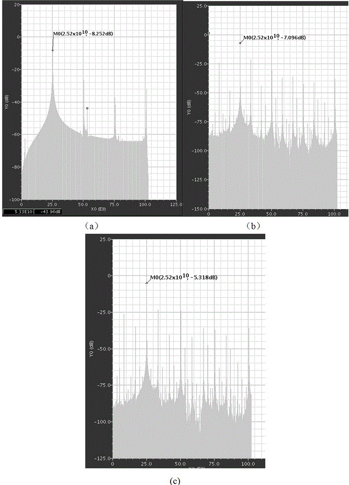
Figure 3
Abstract
Description
technical field
[0001] The invention belongs to the technical field of integrated circuits, and in particular relates to an injection-enhanced low-power-consumption and wide-locking-range injection-locked frequency tripler (Injection Locked Frequency Tripler, ILFT) applied to a radio frequency synthesizer. Background technique
[0002] In millimeter-wave communication, there are two ways to generate local oscillator signals: the first method uses a phase-locked loop directly operating at the required frequency to provide local oscillator signals; the second method uses a low-frequency phase-locked loop followed by a multiplier Frequency converter to provide local oscillator signal. The most important part of the phase-locked loop is the design of the voltage-controlled oscillator (VCO). If the first method of generating local oscillator signals is adopted, it is difficult to design a A high-performance voltage-controlled oscillator (VCO) that meets the requirements of the c...
Examples
Embodiment Construction
[0024] Take the design of an injection-locked frequency tripler with low power consumption and a wide locking range from 21GHz to 26.1GHz as an example.
[0025] Design the circuit diagram as figure 2 As shown, the TSMC 65nm RF CMOS 1P9M process is used, the simulation tool is CadenceSpectreRF, and the power supply voltage is 1.2V. The DC bias of the harmonic generator is about 0.35V, and the DC bias of the bypass current source is about 0.7V.
[0026] The MOS tubes are all radio frequency MOS tubes, the resistors are high-resistance polysilicon resistors, the capacitors are MIM capacitors, the inductors are on-chip spiral inductors with center taps, and the ninth layer of metal wiring.
[0027] The input signal size is 1.9dBm (single-ended peak-to-peak value is 0.7mV) differential signal, the locking range is 21GHz-26.1GHz, and the maximum DC power consumption is 5.28mA.
[0028] image 3 It is the output spectrum diagram obtained by simulation, wherein (a) the spectrum di...