
An al/ge for phase-change memory 10 sb 90 Superlattice-like phase-change thin film material and preparation method
A phase change memory and thin film material technology, applied in the field of microelectronics, can solve problems such as unsatisfactory thermal stability of storage materials, and achieve the effects of low power consumption, shortened operation time, and high speed
Patent Information
- Authority / Receiving Office
- CN · China
- Patent Type
- Patents(China)
- Current Assignee / Owner
- Publication Date
- 2019-11-12
Smart Images
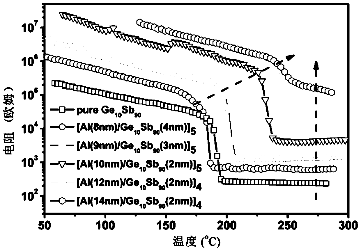
Figure 1 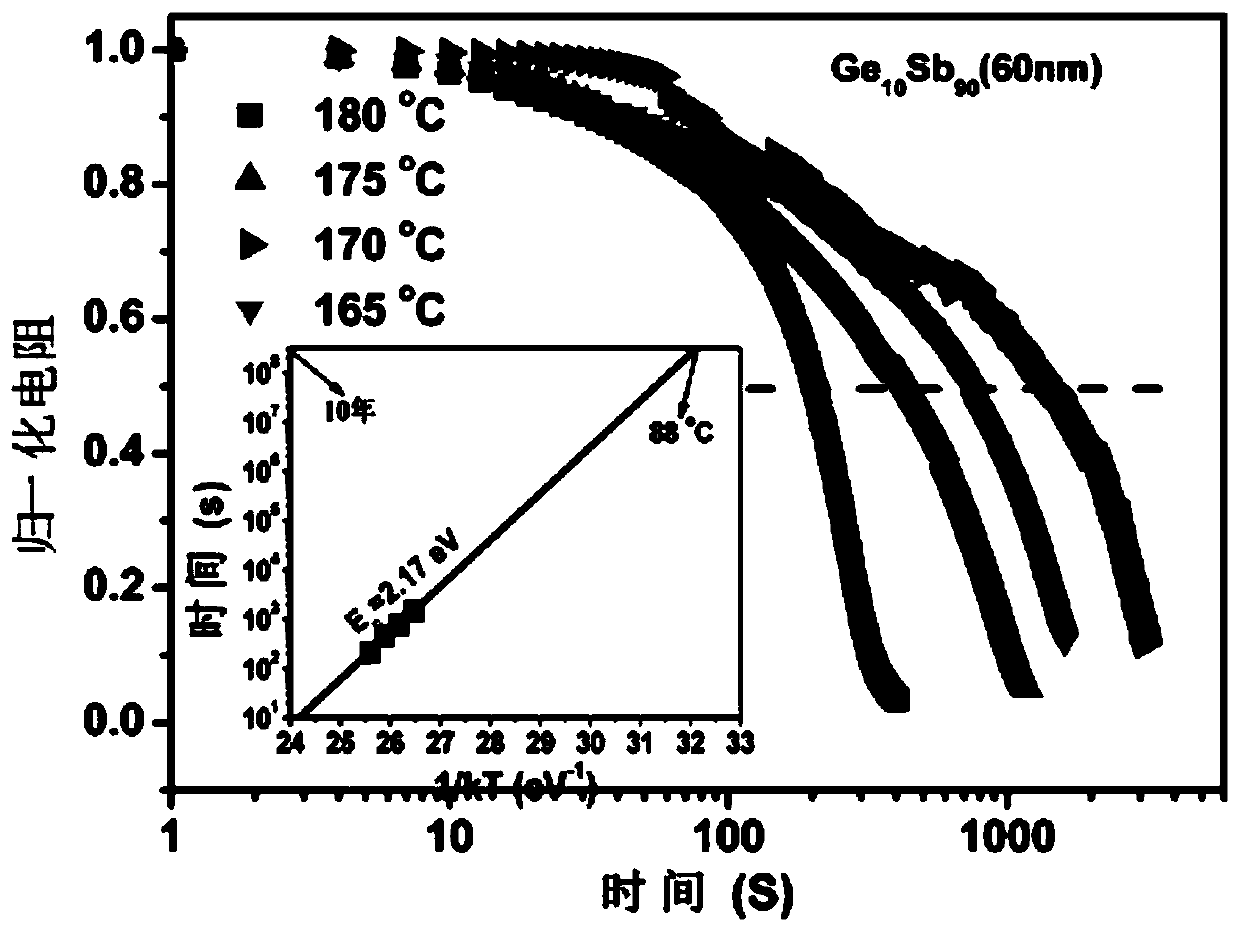
Figure 2 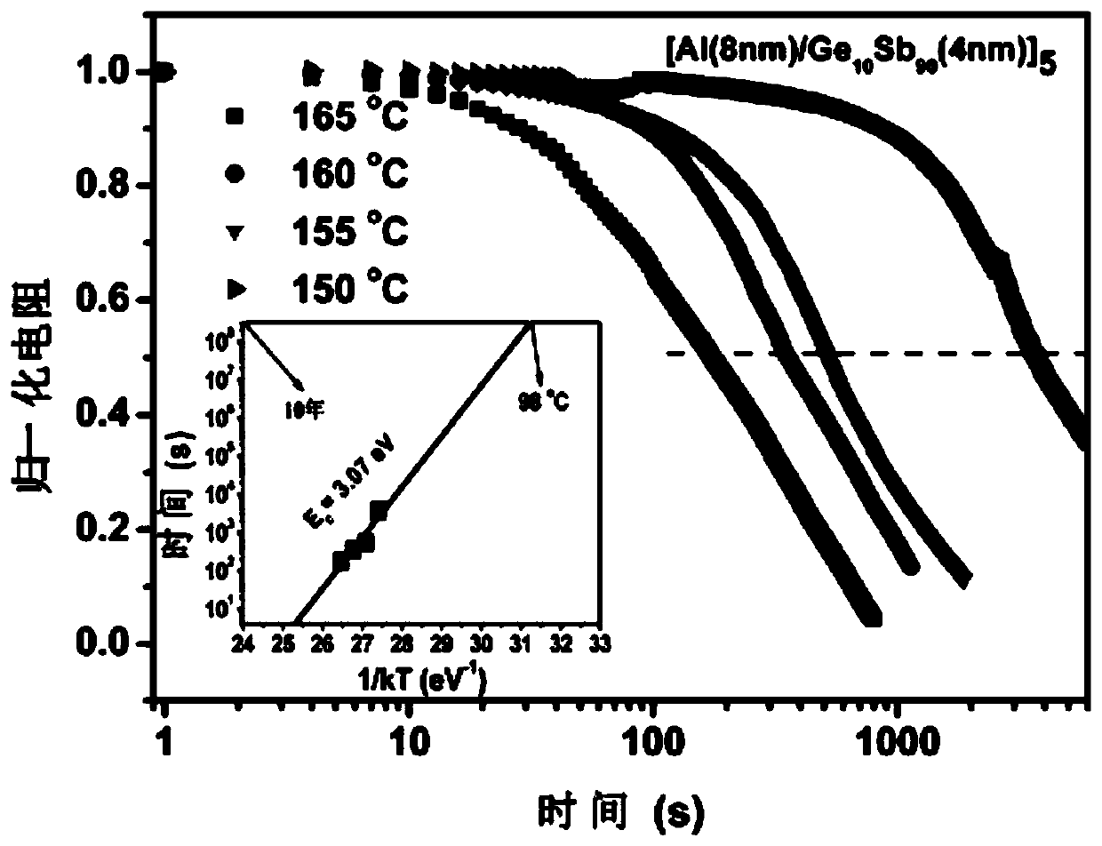
Figure 3
Abstract
Description
technical field
[0001] The invention belongs to the field of microelectronics phase change materials and preparation methods thereof, in particular to a kind of Al / Ge used for phase change memory 10 Sb 90 Superlattice-like phase-change thin film material and preparation method thereof. Background technique
[0002] Memory occupies an important position in the semiconductor market. Only DRAM (dynamnicRandamAccessMemory) and FLASH occupy 15% of the entire market. With the gradual popularization of portable electronic devices, the market for non-volatile memory is also growing. The mainstream of volatile memory, about 90%. However, with the advancement of semiconductor technology, FLAH has encountered more and more technical bottlenecks. First, the floating gate that stores charges cannot be thinned indefinitely with the development of integrated circuit technology. In addition, some other shortcomings of FLASH technology also limit his. application.
[0003] Phase change m...
Examples
Embodiment 1
[0036] Al / Ge of this embodiment 10 Sb 90 The film structure of the superlattice-like phase change thin film material is [Al(8nm)Ge 10 Sb 90 (4nm)] 5 , that is, the thickness of each layer of Al layer is 8nm, each layer of Ge 10 Sb 90 layer thickness is 4nm, Al layer and Ge 10 Sb 90 The number of alternating periods of layers is 5, [Al(8nm)Ge 10 Sb 90 (4nm)] 5 The thickness of the superlattice phase change film material is 60nm.
[0037] [Al(8nm)Ge of the present embodiment 10 Sb 90 (4nm)] 5 The superlattice phase change thin film material is prepared by magnetron sputtering, and the specific preparation method includes the following steps:
[0038] ① Substrate preparation.
[0039] Select SiO with a size of 5mm×5mm 2 / Si (100) substrate, the substrate is ultrasonically cleaned in acetone (a purity of more than 99%) in an ultrasonic cleaning machine for 3 to 5 minutes, and after washing, it is taken out and rinsed with deionized water; then in an ultrasonic clean...
Embodiment 2
[0050] Al / Ge of this embodiment 10 Sb 90 The film structure of the superlattice-like phase change thin film material is [Al(9nm)Ge 10 Sb 90 (3nm)] 5 , that is, the thickness of each layer of Al layer is 9nm, each layer of Ge 10 Sb 90 layer thickness is 3nm, Al layer and Ge 10 Sb 90 The number of alternating periods of layers is 5, [Al(9nm)Ge 10 Sb 90 (3nm)] 5 The thickness of the superlattice phase change film material is 60nm.
[0051] The rest of the preparation method is the same as in Example 1, except that: in the preparation of ② magnetron sputtering, the Ar gas flow rate is set to 30SCCM, and the argon sputtering pressure is adjusted to 0.25Pa, and the sputtering of the radio frequency power supply is set The transmit power is 28W. In step 3. b, the sputtering rate of the Al layer is 4s / nm, and the sputtering time is 18s; in the step 3. c, Ge 10 Sb 90 The layer sputtering rate is 3s / nm and the sputtering time is 9s.
Embodiment 3
[0053] Al / Ge of this embodiment 10 Sb 90 The film structure of the superlattice-like phase change thin film material is [Al(10nm)Ge 10 Sb 90 (2nm)] 5 , that is, the thickness of each layer of Al layer is 10nm, each layer of Ge 10 Sb 90 layer thickness is 2nm, Al layer and Ge 10 Sb 90 The number of alternating periods of layers is 5, [Al(10nm)Ge 10 Sb 90 (2nm)] 5 The thickness of the superlattice phase change film material is 60nm.
[0054] The rest of the preparation method is the same as in Example 1, except that: in the preparation of ② magnetron sputtering, the Ar gas flow rate is set to 35SCCM, and the argon sputtering pressure is adjusted to 0.25Pa, and the sputtering of the radio frequency power supply is set The transmitting power is 30W.
[0055] In the step 3. b, the sputtering rate of the Al layer is 5s / nm, and the sputtering time is 20s; in the step 3. c, the Ge 10 Sb 90 The layer sputtering rate is 4s / nm, and the sputtering time is 6s.