
Fourier stacked microscopy imaging device and method
A Fourier stacking, microscopic imaging technology, applied in microscopes, measuring devices, instruments, etc., can solve the problems of low resolution and low efficiency of restoring sample images, achieve high resolution, easy large-angle illumination, modulation Efficient effect
Patent Information
- Authority / Receiving Office
- CN · China
- Patent Type
- Patents(China)
- Current Assignee / Owner
- Publication Date
- 2020-11-17
Smart Images
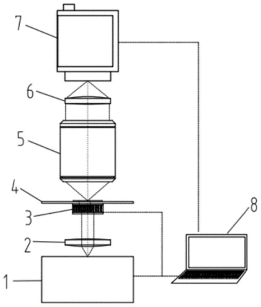
Figure 1 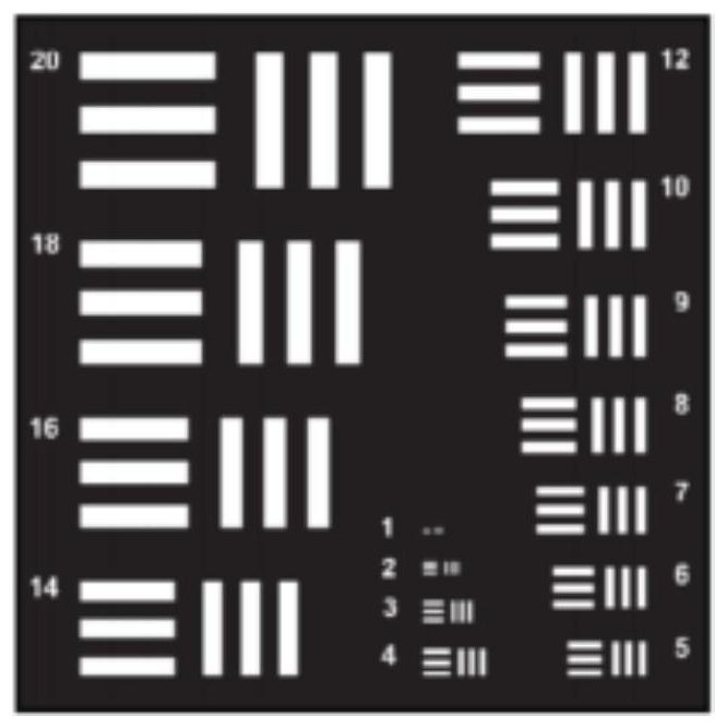
Figure 2 
Figure 3
Abstract
Description
technical field
[0001] The invention belongs to the technical field of optical microscopic imaging, and relates to Fourier stacked microscopic imaging technology, in particular to a Fourier stacked microscopic imaging device and method based on liquid crystal beam deflection technology. Background technique
[0002] Traditional optical microscopes cannot obtain large field of view and high-resolution images at the same time, and can only obtain the amplitude information of the sample, but cannot obtain the phase information.
[0003] In 2013, Zheng from Caltech introduced Fourier stack imaging technology into the field of microscopic imaging for the first time, and realized microscopic imaging technology with high resolution and large field of view at the same time: by placing the LED array at a certain distance below the sample , the thin sample on the sample stage is illuminated by different angles of plane light from different LEDs, on the Fourier plane of the microscope ...
Examples
Embodiment
[0102] The liquid crystal beam deflection device 3 adopts a liquid crystal prism;
[0103] The microscopic objective lens 5 adopts a twice achromatic microscopic objective lens, the numerical aperture NA is 0.1, and the objective lens aperture is 15mm;
[0104] The sample to be tested (such as figure 2 ) is the USAF1951 standard resolution board;
[0105] Laser 1 selects a red He-Ne laser with a wavelength of 632nm;
[0106] Collimating lens 2 collimates the laser beam to the parallel light;
[0107] Camera 7 uses a CCD sensor with a pixel size of 5.5um;
[0108] The liquid crystal prism is placed close to the bottom of the sample stage 4;
[0109] The desired synthetic numerical aperture NA' is 0.3, and it is necessary to ensure that the spectral overlap ratio = 50%.
[0110] Follow the steps below to implement:
[0111] The first step: determine the beam angle α of each modulation of the liquid crystal prism i,j .
[0112] 1.1 According to N=2NA' / NA, calculate N=6...