
Display panel and display device
a display panel and display technology, applied in the field of display technology, can solve problems such as the reduction of the aperture ratio of the pixel uni
Patent Information
- Authority / Receiving Office
- US · United States
- Current Assignee / Owner
- Publication Date
- 2022-09-29
Smart Images
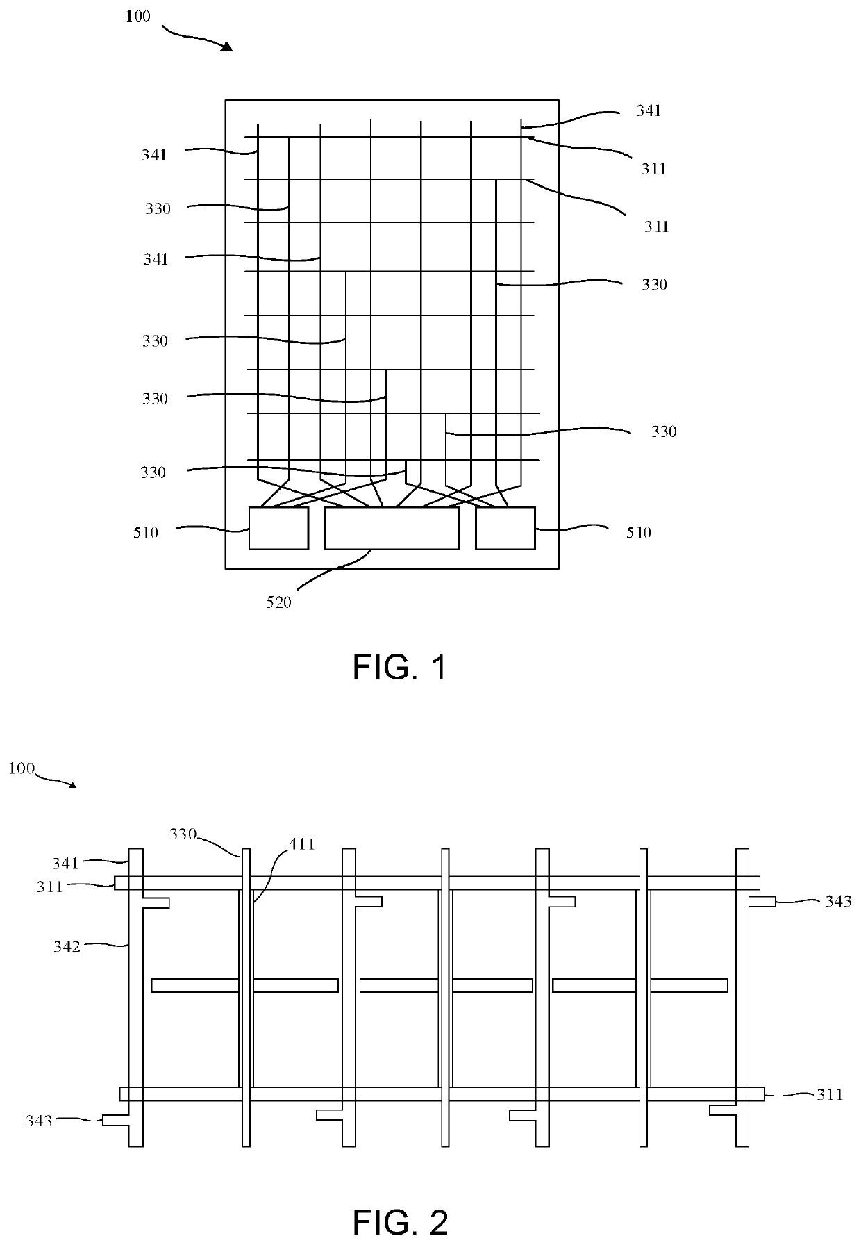
Figure 1 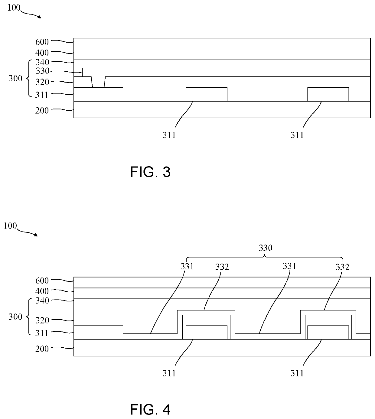
Figure 2 
Figure 3
Abstract
Description
FIELD OF INVENTION
[0001] The present disclosure relates to the field of display technology, and more particularly, to a display panel and a display device.BACKGROUND OF INVENTION
[0002] With improvement of living standards, people's demand for display screens with narrow frames and high aperture ratio is becoming increasingly higher.
[0003] In the prior art, scanning signal line transmission lines are arranged between adjacent pixel units in a display region of display panels, which increase a distance between adjacent pixel units, resulting in a decrease in aperture ratio of the pixel units.
[0004] Thus, a display panel and a display device are urgently needed to solve the above technical problems.SUMMARY OF INVENTION
[0005] The present disclosure provides a display panel and a display device to solve the technical problems in the prior art that scanning signal line transmission lines are arranged between adjacent pixel units in a display region of display panels, which increases a distance...
Examples
Embodiment Construction
[0035]The present disclosure provides a display panel and a display device. In order to make purposes, technical solutions, and effects of the present disclosure clearer and more definite, following describes the present disclosure in detail with reference to the drawings and examples. It should be understood that specific embodiments described herein are only used to explain the present disclosure, and are not intended to limit the present disclosure.
[0036]Refer to FIG. 1 to FIG. 6, the present disclosure provides a display panel 100, the display panel 100 comprises a first substrate 200, a driving circuit layer 300 located on the first substrate 200, and a first common electrode layer 400 located on the driving circuit layer 300.
[0037]The display panel 100 further comprises at least one scanning signal transmission line 330 located between two adjacent data lines 341 and arranged in parallel with the data lines 341, and one of the scanning signal transmission lines 330 is connecte...