
Surface mount crystal oscillator
a crystal oscillator and surface mount technology, applied in the field of crystal oscillators, can solve the problems of high oscillation frequency of oscillators, achieve good oscillation characteristics, facilitate a reduction in size, and suppress the occurrence of stress
Patent Information
- Authority / Receiving Office
- US · United States
- Patent Type
- Patents(United States)
- Current Assignee / Owner
- Publication Date
- 2008-03-04
- Estimated Expiration
- Not applicable · inactive patent
Smart Images
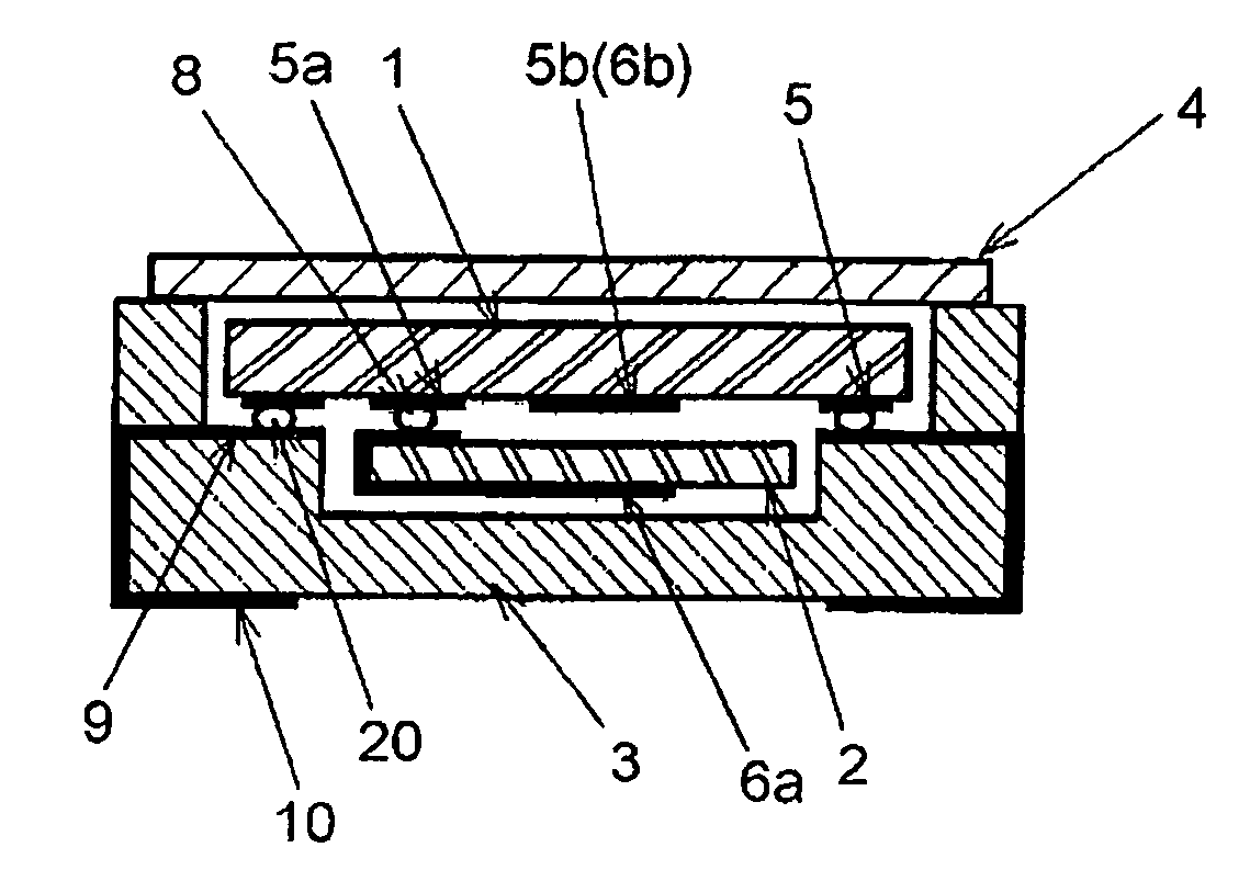
Figure 1 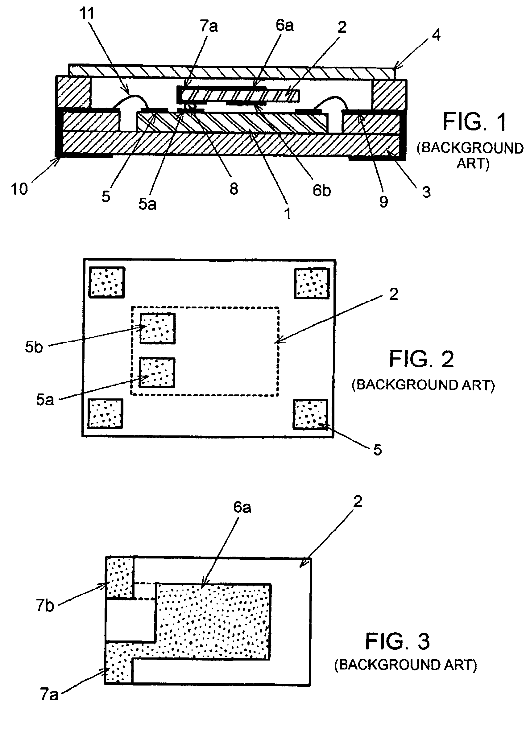
Figure 2 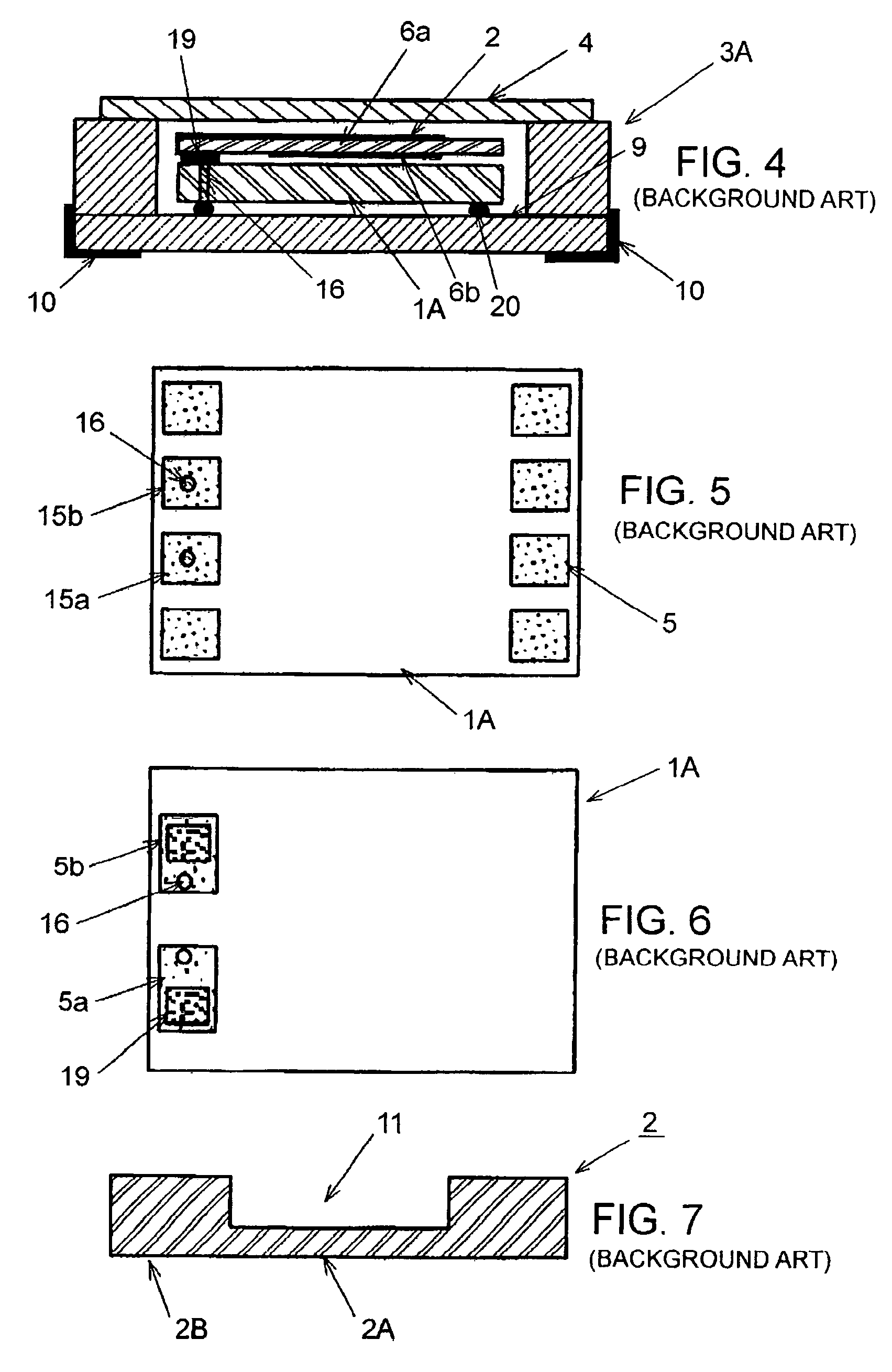
Figure 3
Abstract
Description
BACKGROUND OF THE INVENTION
[0001] 1. Field of the Invention
[0002] The present invention relates to a crystal oscillator of a surface mount type, and more particularly, to a miniature surface mount crystal oscillator which has a crystal blank mounted on an IC (integrated circuit) chip.
[0003] 2. Description of the Related Art
[0004] A crystal oscillator which includes a quartz crystal unit and an oscillation circuit using the crystal unit integrated therein is used as a reference source for the frequency and time in a variety of devices. Particularly, surface mount crystal oscillators are contained in portable electronic devices as a reference source for the frequency and time because of its small size and light weight. In recent years, the oscillation frequency of surface mount crystal oscillators is made increasingly higher, driven by ever widespreading optical communications systems as well, to reach even into a 600 MHz band.
[0005] A further reduction in size as well as a higher oscillat...
Examples
first embodiment
[0042]FIG. 8 illustrates a surface mount crystal oscillator according to the present invention. In the following description, components identical to those inFIGS. 1 to 7 are designated the same reference numerals, and repetitive descriptions thereon will be simplified.
[0043]The surface mount crystal oscillator of the first embodiment comprises surface mount package body 3 similar to the package body in the crystal oscillator illustrated in FIG. 1; IC chip 1 and crystal blank 2 integrated and contained in a recess of package body 3; and a cover 4 put on package body 3 to hermetically encapsulate IC chip 1 and crystal blank 2.
[0044]IC chip 1 has an oscillation circuit, which uses crystal blank 2, and the like integrated therein. On a circuit forming surface of IC chip 1 formed with circuits such as the oscillation circuit, a plurality of IC terminals 5, including a power supply terminal, a ground terminal, and an output terminal, are disposed at four corners of the circuit forming su...
second embodiment
[0061]In the surface mount crystal oscillator of the second embodiment described above, cavity 12 is formed on the other principal surface of crystal blank 2 to ensure the spacing between the vibration region of crystal blank 2 and the back side of IC chip A. Alternatively, the total thickness of crystal connection terminal 5a and eutectic alloy 19 may be controlled, or crystal connection terminal 5a may be increased in thickness, or a spacer may be provided, instead of providing cavity 12. However, the spacing between the vibration region and IC chip 1A can be maintained with certainty when cavity 12 is provided.