
Embedded nano UV blocking and diffusion barrier for improved reliability of copper/ultra low K interlevel dielectric electronic devices
a technology of low-k-interferometer and nano-uv blockage, which is applied in the direction of semiconductor devices, semiconductor/solid-state device details, electrical apparatus, etc., can solve the problems of copper diffused easily into the surrounding dielectric material, the uv/e-beam modification is prevented, and the device scale is decreased. , to achieve the effect of reducing the dielectric constant, minimizing the stress change, and preventing the modification of uv/e-beam
Patent Information
- Authority / Receiving Office
- US · United States
- Patent Type
- Patents(United States)
- Current Assignee / Owner
- Publication Date
- 2010-07-06
- Estimated Expiration
- Not applicable · inactive patent
Smart Images
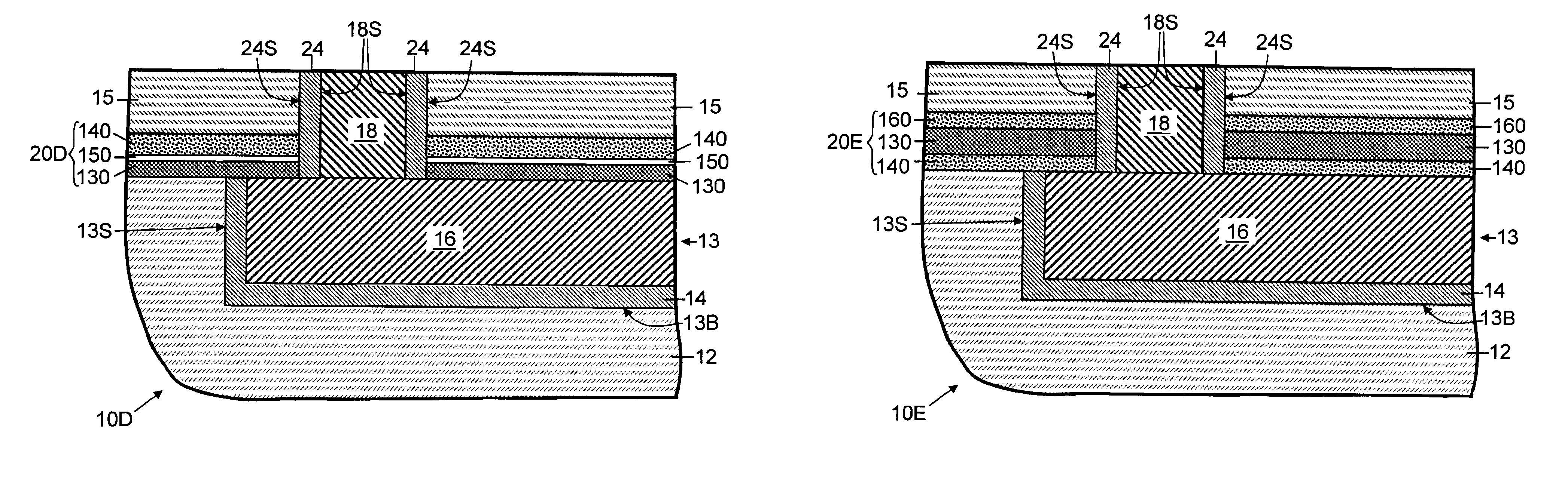
Figure 1 
Figure 2 
Figure 3
Abstract
Description
BACKGROUND OF THE INVENTION
[0001] The present invention relates to protection of the interconnection structures, known as interconnects, in Ultra-Large Scale Integrated (ULSI) microelectronic circuits including high speed microprocessors, application specific integrated circuits, memory storage devices, and related electronic structures with a multilayered barrier layer. More particularly this invention relates to the structure of cap layers for protecting interconnect-metallization in Back End Of Line (BEOL) structures in such ULSI microelectronic circuits.
[0002] In traditional semiconductor devices, aluminum and aluminum alloys have been used as interconnect metallurgies for providing electrical connections to and from devices in BEOL layers of the devices. While aluminum-based metallurgies have been the material of choice for use as metal interconnects in the past, aluminum no longer satisfies requirements as circuit density and speeds for semiconductor devices increase and the sca...
Examples
Embodiment Construction
[0059]In one embodiment of the present invention, a multilayered diffusion barrier layer is thermally stable above 300° C., has a thickness between 10 nm and 50 nm, and is comprised of at least two laminated films, i.e. a dual film (bilayer), where at least one film is an air and metal diffusion barrier and at least another of the dual films is a UV blocking film. The multi-film diffusion barrier layer of the present invention may have a variety of configurations including, for example, dual films with the UV blocking film atop the laminated cap barrier, dual films with the cap barrier film atop the UV blocking film, or a triple film (three laminated films or which may be referred to as a trilayer) with the UV blocking film placed between two cap barrier films. For example, (a) if the objective is to prevent UV penetration, the UV blocking film is deposited on top; (b) if the objective is to allow partial UV penetration, the film is inserted in middle of a triple film; and (c) if th...