
Resonator tunnel device
a tunnel device and resonator technology, applied in the field of resonators, can solve the problems of limiting the configuration of the resonator to achieve impedance matching, the thickness and/or the material of the dielectric included in the resonator, and the difficulty of selecting the thickness and/or the material of the resonator, so as to reduce the delay time, reduce the delay time (rc time constant) and reduce the delay time
Patent Information
- Authority / Receiving Office
- US · United States
- Patent Type
- Patents(United States)
- Current Assignee / Owner
- Publication Date
- 2012-11-27
Smart Images
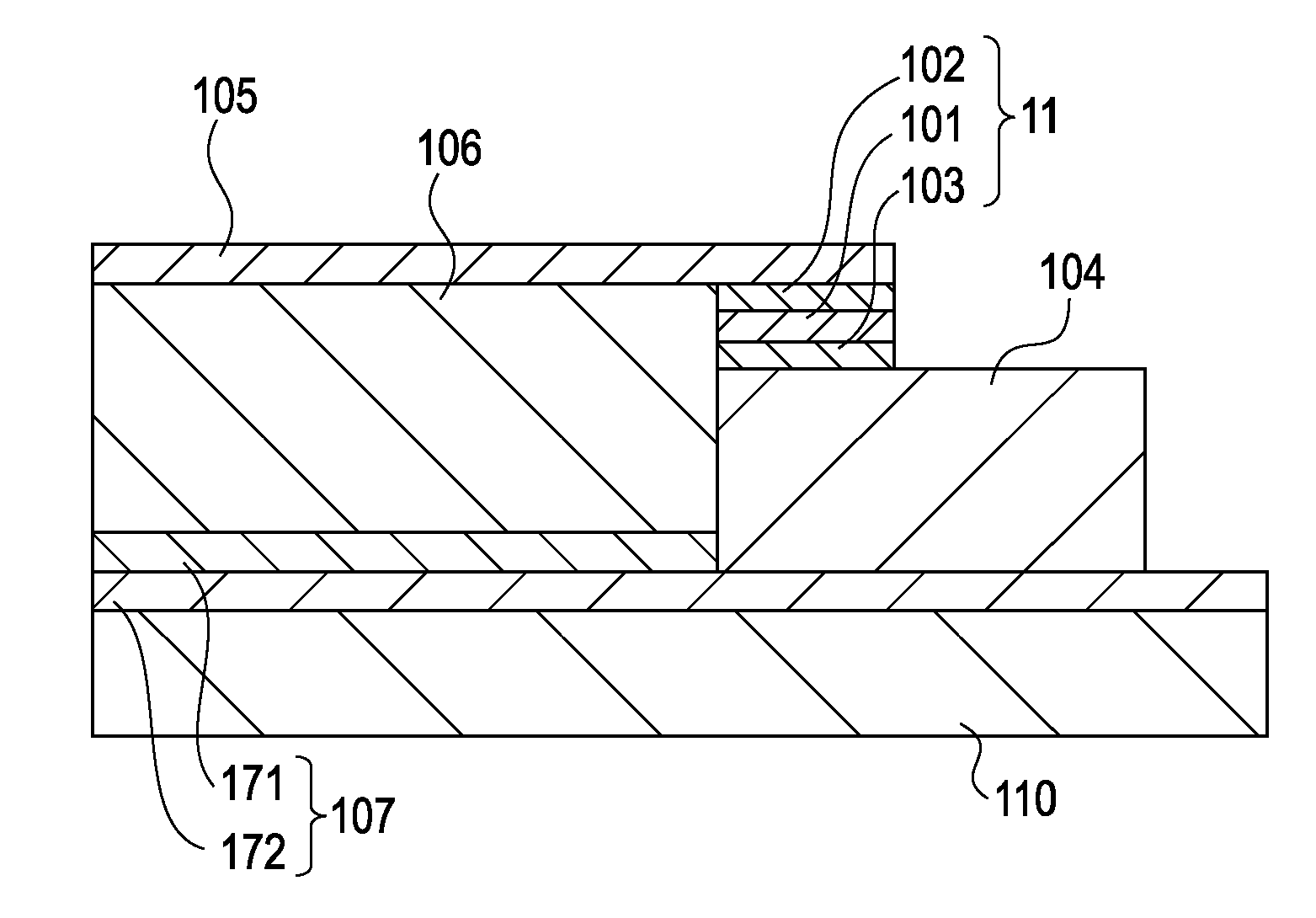
Figure 1 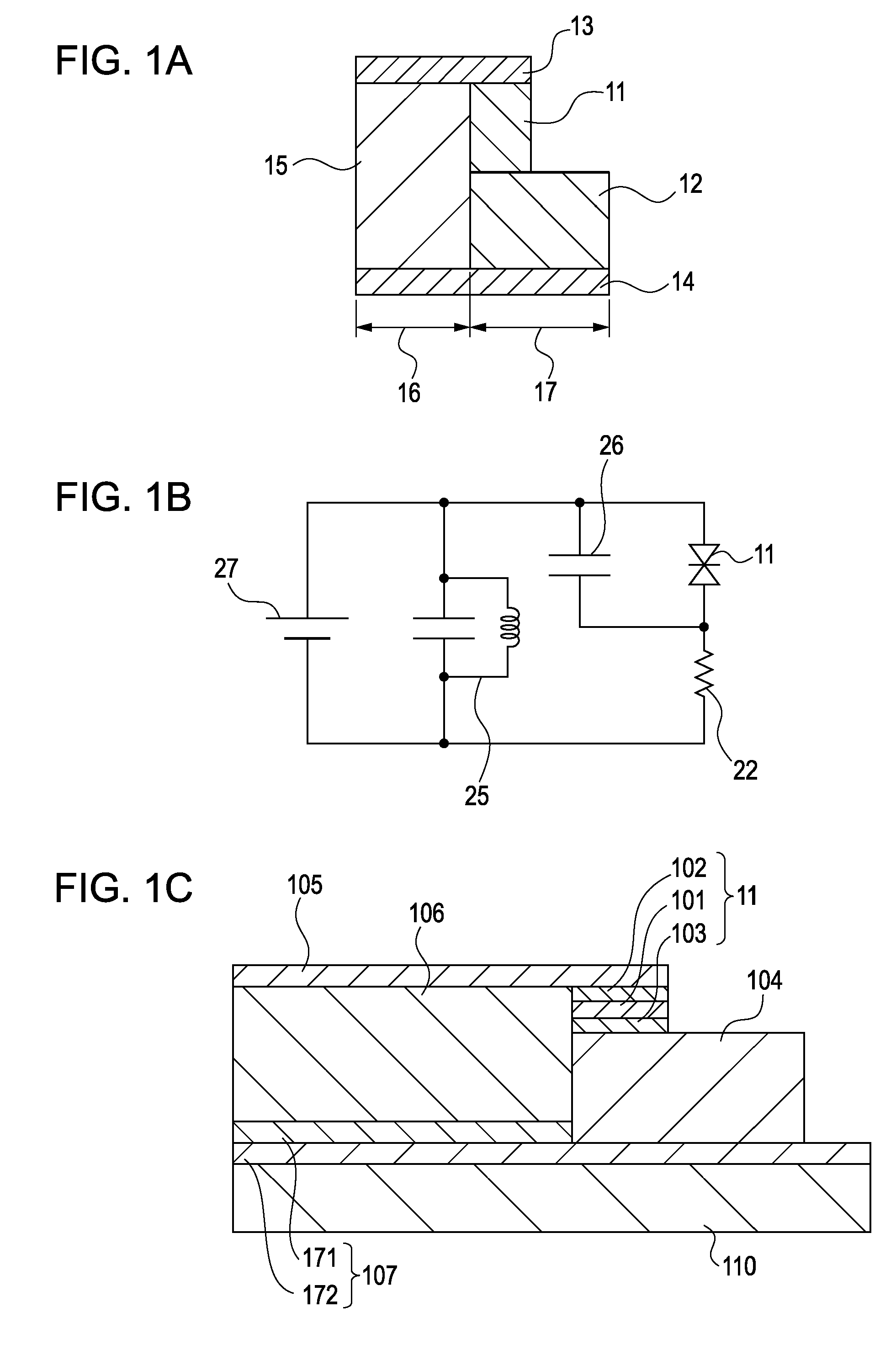
Figure 2 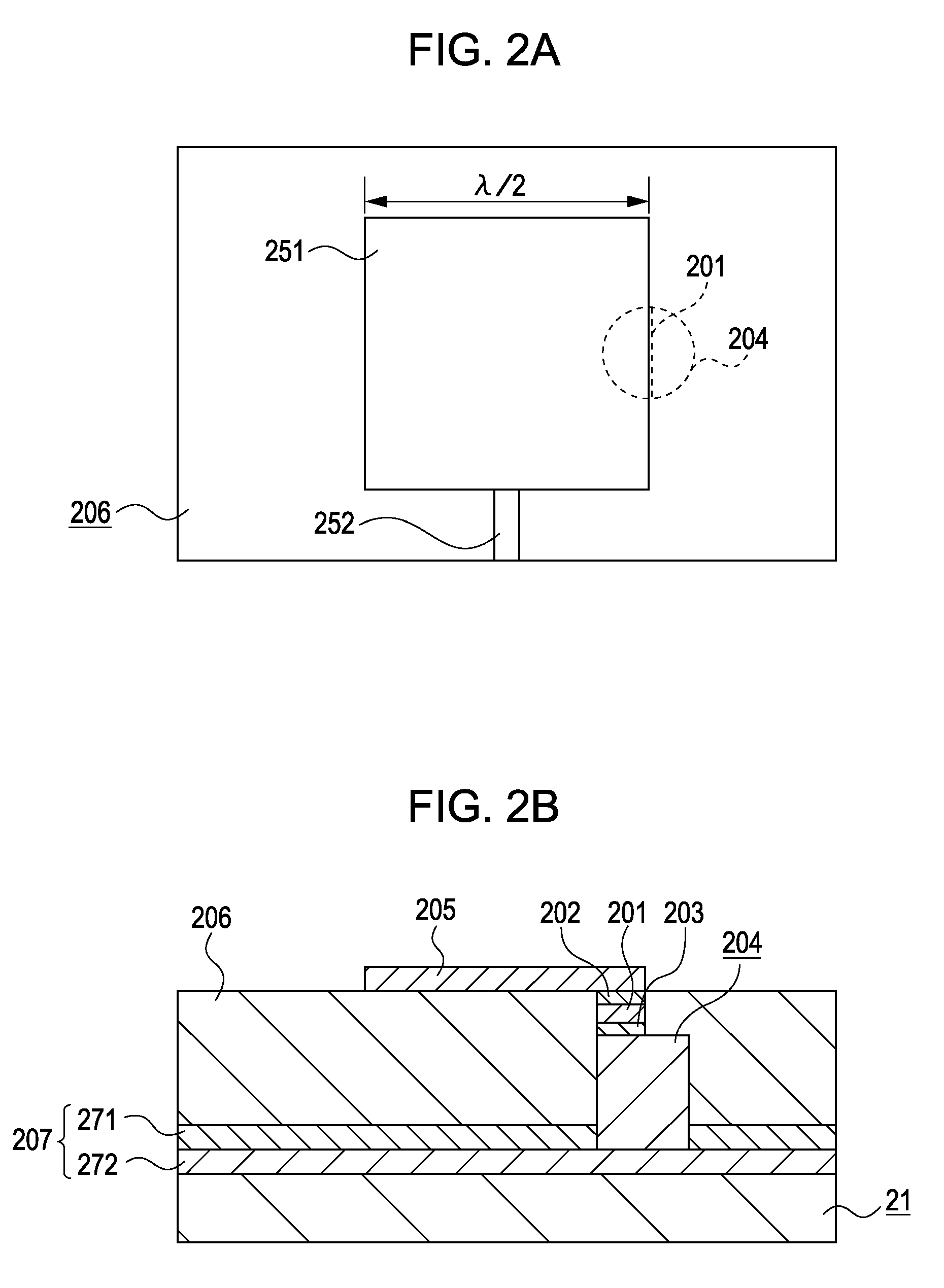
Figure 3
Abstract
Description
BACKGROUND OF THE INVENTION
[0001] 1. Field of the Invention
[0002] The present invention relates to a resonator including a resonant tunneling diode (RTD) configured to generate an electromagnetic wave.
[0003] 2. Description of the Related Art
[0004] It has been widely recognized that electronegative resistance elements include a resonator and can be applied for an electromagnetic wave generator. Hitherto, it has been recognized that the electronegative resistance element generates an electromagnetic wave (also referred to as a terahertz wave in this specification) including at least part of frequencies falling within a frequency band of from a millimeter wave band to a terahertz wave band inclusive (from 30 GHz to 30 THz inclusive).
[0005] As an example of the electronegative resistance elements, a monolithic resonator including a semiconductor substrate including the RTD, a microstrip conductor, and a grounding conductor, where the semiconductor substrate is sandwiched between the microstr...
Examples
first embodiment
[0039]A resonator according to a first embodiment of the present invention will be described with reference to FIG. 1C. FIG. 1C shows a sectional view of the resonator of the first embodiment.
[0040]An RTD according to the first embodiment includes a resonant tunneling structure layer 101, the electrical contact layers 102 and 103 (first and second electrical contact layers 102 and 103) that are provided to apply a current to the resonant tunneling structure layer 101, and a resistor layer 104. The resonator of the first embodiment includes two conductors 105 and 107 that are opposed to each other (first and second conductors 105 and 107), and a dielectric 106 provided between the two conductors 105 and 107. The resonant tunneling structure layer 101 is connected to a grounded metal 171 via a metal contact layer 172, and the conductor 107 (the grounded metal 171 and the grounded metal layer 172) doubles as a common electrode provided for a direct current (DC) and an alternating curre...
second embodiment
Microstrip Antenna
[0046]A resonator according to a second embodiment of the present invention will be described with reference to FIGS. 2A and 2B. FIG. 2A is the top plan view of the resonator of the above-described embodiment and FIG. 2B is the sectional view of the resonator of the above-described embodiment. The resonator of the above-described embodiment includes a patch antenna which is widely known as a microstrip antenna. The patch antenna is a distributed constant resonator and the resonance frequency thereof is determined based on the in-plane length of a patch antenna 251. Usually, a λ / 2 patch antenna is used. An electromagnetic wave emitted from a resonant tunneling diode is caused to resonate with the patch antenna and oscillates. Then, the electromagnetic wave can be taken outside through the use of the load on the patch antenna 251. Here, the specification of the load on the patch antenna 251 is determined based on a desired output to be taken out. According to an embo...
third embodiment
Microstrip Filter
[0049]A resonator according to a third embodiment of the present invention will be described with reference to FIGS. 3A and 3B. FIG. 3A is the top plan view of the resonator of the above-described embodiment and FIG. 3B is the sectional view of the resonator of the above-described embodiment. The resonator of the above-described embodiment includes a coupled-line filter widely known as a microstrip filter. The coupled-line filter is a distributed constant resonator and the resonance frequency thereof (specified frequency) is determined based on the in-plane length of a microstrip-line resonator 351. Usually, a λ / 2 microstrip line is used. Further, two microstrip lines 308 are provided to have a magnetic field coupling with the λ / 2 microstrip line. An electromagnetic wave emitted from a resonant tunneling diode is injection-synchronized with an electromagnetic wave transmitted to one of the microstrip lines 308 and oscillates. In this manner, an electromagnetic wave ...