

3D DRAM vs Doping-Based 3D Memory: Insights
APR 15, 20269 MIN READ
Generate Your Research Report Instantly with AI Agent
PatSnap Eureka helps you evaluate technical feasibility & market potential.
3D Memory Architecture Evolution and Technical Objectives
The evolution of three-dimensional memory architectures represents a paradigm shift from traditional planar semiconductor designs to vertically stacked structures, fundamentally addressing the physical limitations imposed by Moore's Law scaling challenges. This architectural transformation emerged from the industry's recognition that continued miniaturization in two-dimensional space would eventually encounter insurmountable technical and economic barriers, necessitating exploration of the third dimension for memory density improvements.
Traditional memory architectures relied heavily on lateral scaling, where transistor dimensions were continuously reduced to achieve higher density and performance. However, as feature sizes approached atomic scales, quantum effects, manufacturing complexity, and cost escalation became prohibitive factors. The transition to 3D architectures began with NAND flash memory in the early 2010s, demonstrating the viability of vertical stacking approaches and establishing foundational principles for subsequent 3D memory developments.
The architectural evolution encompasses two primary technological pathways: conventional 3D DRAM structures that extend traditional charge-based storage mechanisms into vertical configurations, and innovative doping-based 3D memory systems that leverage material property modifications for information storage. These approaches represent fundamentally different philosophies in addressing scalability challenges while maintaining compatibility with existing semiconductor manufacturing ecosystems.
3D DRAM architectures focus on vertically stacking conventional capacitor-transistor pairs, utilizing through-silicon vias and advanced interconnect technologies to maintain electrical connectivity across multiple layers. This approach preserves familiar DRAM operational characteristics while achieving significant density improvements through layer multiplication rather than feature size reduction.
Conversely, doping-based 3D memory architectures exploit controlled impurity introduction within semiconductor substrates to create discrete storage regions with distinct electrical properties. This methodology enables ultra-high density storage by utilizing atomic-level modifications rather than traditional geometric scaling, potentially achieving storage densities several orders of magnitude beyond conventional approaches.
The technical objectives driving these architectural developments include achieving storage densities exceeding 1 terabit per cubic centimeter, maintaining sub-nanosecond access times comparable to current DRAM performance standards, and ensuring manufacturing compatibility with existing semiconductor fabrication infrastructure. Additionally, power efficiency improvements, thermal management optimization, and cost-per-bit reduction remain critical objectives influencing architectural design decisions.
These evolutionary trajectories reflect the industry's strategic response to fundamental physical limitations, establishing new technological foundations for next-generation memory systems capable of supporting increasingly demanding computational workloads and data-intensive applications across diverse market segments.
Market Demand Analysis for Advanced 3D Memory Solutions
The global memory market is experiencing unprecedented demand driven by the exponential growth of data-intensive applications across multiple sectors. Cloud computing infrastructure, artificial intelligence workloads, and high-performance computing systems require memory solutions that can deliver superior density, speed, and energy efficiency. Traditional planar memory architectures are approaching physical scaling limits, creating a critical need for three-dimensional memory technologies that can overcome these constraints.
Enterprise data centers represent the largest segment driving advanced 3D memory adoption. These facilities require massive memory capacity to support virtualization, real-time analytics, and machine learning operations. The shift toward in-memory computing architectures has intensified demand for high-density memory solutions that can maintain data persistence while delivering DRAM-like performance characteristics.
Mobile and edge computing applications constitute another significant demand driver for advanced 3D memory technologies. Smartphones, tablets, and IoT devices require memory solutions that balance high performance with stringent power consumption requirements. The proliferation of 5G networks and edge AI processing capabilities has created new performance benchmarks that traditional memory architectures struggle to meet efficiently.
Automotive electronics and autonomous vehicle systems are emerging as high-growth market segments for 3D memory solutions. Advanced driver assistance systems, infotainment platforms, and autonomous driving algorithms require reliable, high-performance memory that can operate under extreme environmental conditions while processing vast amounts of sensor data in real-time.
The gaming and graphics processing market continues to drive demand for high-bandwidth memory solutions. Modern gaming applications, virtual reality systems, and professional graphics workstations require memory architectures that can support increasingly complex visual processing tasks and real-time rendering operations.
Industrial automation and smart manufacturing applications are creating new market opportunities for specialized 3D memory solutions. These systems require memory technologies that can deliver consistent performance in harsh industrial environments while supporting real-time control systems and predictive maintenance algorithms.
Market analysis indicates that both 3D DRAM and doping-based 3D memory technologies address distinct segments of this growing demand landscape, with each technology offering unique advantages for specific application requirements and performance criteria.
Current Status and Challenges in 3D DRAM vs Doping Technologies
The current landscape of 3D memory technologies presents a complex competitive environment between traditional 3D DRAM architectures and emerging doping-based 3D memory solutions. 3D DRAM technology has achieved significant commercial success, with major manufacturers like Samsung, SK Hynix, and Micron successfully implementing vertical stacking approaches that utilize through-silicon vias (TSVs) and advanced packaging techniques. These implementations have demonstrated the ability to achieve higher memory densities while maintaining compatibility with existing memory controllers and system architectures.
However, 3D DRAM faces substantial technical constraints that limit its scalability potential. The primary challenge lies in the inherent complexity of maintaining signal integrity across multiple stacked layers, particularly as the number of vertical tiers increases. Thermal management becomes increasingly problematic with higher stack counts, as heat dissipation from inner layers creates performance bottlenecks and reliability concerns. Additionally, the manufacturing yield decreases significantly with increased layer complexity, driving up production costs and limiting economic viability for ultra-high-density applications.
Doping-based 3D memory technologies, including resistive RAM (ReRAM), phase-change memory (PCM), and ferroelectric RAM (FeRAM), represent alternative approaches that leverage material property modifications rather than traditional charge storage mechanisms. These technologies demonstrate superior scalability potential, with the ability to create truly three-dimensional memory cells within individual layers rather than simply stacking planar structures. The doping-based approaches also exhibit lower power consumption characteristics and faster switching speeds compared to conventional DRAM architectures.
The primary challenges facing doping-based 3D memory technologies center around manufacturing consistency and long-term reliability. Precise control of doping concentrations across large wafer areas remains technically demanding, with variations in material properties leading to inconsistent memory cell performance. Endurance limitations, particularly in write-erase cycles, continue to constrain the applicability of these technologies in high-frequency access scenarios. Furthermore, the integration of doping-based memory cells with existing semiconductor manufacturing processes requires significant modifications to established production lines.
Current market adoption patterns reveal a geographical concentration of 3D DRAM development primarily in South Korea, Taiwan, and select facilities in the United States, while doping-based memory research shows broader distribution across academic institutions and emerging technology companies globally. The maturity gap between these technologies creates distinct market positioning opportunities, with 3D DRAM serving immediate high-performance computing needs and doping-based solutions targeting future ultra-dense storage applications.
Current Technical Approaches in 3D Memory Implementation
01 3D DRAM architecture with vertical stacking
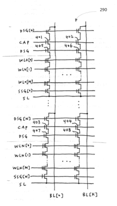
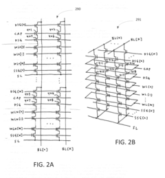
Three-dimensional DRAM structures utilize vertical stacking of memory cells to increase storage density. This approach involves arranging memory cells in multiple layers above the substrate, enabling higher capacity within the same footprint. The vertical architecture includes through-silicon vias and interconnects to facilitate communication between layers, improving overall memory performance and reducing access latency.- 3D DRAM architecture with vertical stacking: Three-dimensional DRAM structures utilize vertical stacking of memory cells to increase storage density. This approach involves arranging memory cells in multiple layers above the substrate, enabling higher capacity within the same footprint. The vertical architecture includes through-silicon vias and interconnects to facilitate communication between layers, improving overall memory performance and reducing latency.
- Doping techniques for 3D memory cell formation: Advanced doping methods are employed to create functional memory cells in three-dimensional structures. These techniques involve selective introduction of dopants into specific regions of the semiconductor material to form transistors and storage elements. The doping process is carefully controlled to achieve desired electrical characteristics while maintaining structural integrity across multiple layers of the memory device.
- Capacitor structures in 3D DRAM configurations: Specialized capacitor designs are implemented in three-dimensional DRAM to maintain charge storage capability while accommodating vertical architecture. These structures include cylindrical, pillar-shaped, or trench capacitors that extend through multiple layers. The capacitor configurations are optimized to maximize capacitance while minimizing cell size, ensuring reliable data retention in high-density memory arrays.
- Access transistor integration in 3D memory: Integration of access transistors in three-dimensional memory involves forming switching elements that control read and write operations for individual memory cells. The transistors are fabricated using vertical channel structures or stacked planar configurations, with precise doping profiles to ensure proper threshold voltages and switching characteristics. This integration enables efficient addressing and data transfer in high-density memory arrays.
- Manufacturing processes for 3D doped memory structures: Fabrication methods for three-dimensional doped memory devices involve sequential deposition, patterning, and etching steps to create multi-layer structures. These processes include atomic layer deposition, chemical vapor deposition, and ion implantation techniques to achieve precise doping profiles. The manufacturing approach addresses challenges such as aspect ratio limitations, uniformity across layers, and thermal budget constraints to produce reliable high-density memory devices.
02 Doping techniques for 3D memory cell formation
Doping-based methods are employed to create functional regions in three-dimensional memory structures. These techniques involve introducing specific impurities into semiconductor materials at precise locations to form source, drain, and channel regions in vertically stacked memory cells. The doping process enables control of electrical properties and threshold voltages, which is critical for reliable memory operation in 3D configurations.Expand Specific Solutions03 Capacitor structures in 3D DRAM cells
Advanced capacitor designs are integrated into three-dimensional DRAM architectures to maintain charge storage capability while minimizing cell size. These structures include vertical capacitors, trench capacitors, and stacked capacitor configurations that are compatible with 3D integration. The capacitor formation process is optimized to achieve high capacitance density and low leakage current in the confined spaces of 3D memory arrays.Expand Specific Solutions04 Access transistor optimization for 3D memory
Access transistors in three-dimensional memory structures are designed with specific doping profiles and geometries to enable efficient cell selection and data access. The optimization includes controlling channel doping concentrations, gate oxide thickness, and transistor dimensions to achieve low off-state leakage and high on-state current. These transistors are integrated with vertical bit lines and word lines to form complete 3D memory arrays.Expand Specific Solutions05 Interconnect and contact formation in 3D memory arrays
Interconnection schemes for three-dimensional memory involve creating vertical and horizontal conductive pathways between stacked memory layers. This includes forming contact plugs, metal lines, and vias using selective doping and metallization processes. The interconnect architecture ensures proper electrical connectivity while maintaining structural integrity across multiple layers, enabling scalable 3D memory integration with reduced parasitic capacitance and resistance.Expand Specific Solutions
Major Players in 3D DRAM and Doping-Based Memory Markets
The 3D DRAM versus doping-based 3D memory landscape represents a rapidly evolving sector within the advanced memory industry, currently in its growth phase with significant technological differentiation emerging. The market demonstrates substantial scale potential, driven by increasing demand for high-density, low-power memory solutions across data centers, mobile devices, and AI applications. Technology maturity varies considerably among key players, with established semiconductor giants like Samsung Electronics, Intel, and Micron Technology leading traditional 3D DRAM development, while companies such as Yangtze Memory Technologies and emerging players like 4DS Memory are pioneering alternative doping-based approaches. Research institutions including Imec and various universities are contributing foundational innovations, while equipment manufacturers like Applied Materials and Tokyo Electron are enabling production scalability, creating a competitive ecosystem where both evolutionary and revolutionary memory architectures compete for market dominance.
Yangtze Memory Technologies Co., Ltd.
Technical Solution: YMTC has developed innovative Xtacking architecture for 3D NAND flash memory, separating peripheral circuits from memory cell arrays to enable independent optimization of both components. Their doping-based 3D memory technology utilizes charge trap flash cells with silicon nitride storage layers and advanced word line replacement techniques. The company has achieved over 128 layers of vertical integration using sophisticated etching processes and innovative staircase structures. YMTC's manufacturing approach incorporates advanced doping techniques for precise threshold voltage control and optimized charge retention characteristics, enabling competitive performance and reliability in high-density storage applications.
Strengths: Innovative Xtacking architecture, rapid technology development, strong government support. Weaknesses: Relatively new market entrant, limited global market presence, geopolitical trade restrictions.
Intel Corp.
Technical Solution: Intel has developed 3D XPoint memory technology combining aspects of both 3D DRAM and doping-based approaches, utilizing chalcogenide glass materials with unique phase-change properties for non-volatile storage. Their architecture employs cross-point arrays with selector devices, achieving storage densities 10x higher than conventional DRAM while maintaining near-DRAM performance characteristics. Intel's 3D memory solutions feature innovative materials engineering including germanium-antimony-tellurium compounds optimized for rapid phase transitions, enabling both high-speed access and persistent data storage capabilities in vertically stacked configurations.
Strengths: Strong materials science expertise, innovative cross-point architecture, excellent performance characteristics. Weaknesses: Manufacturing complexity, limited production scale compared to traditional memory technologies.
Key Patents and Innovations in 3D Memory Architectures
Method and apparatus for providing three-dimensional integrated nonvolatile memory (NVM) and dynamic random access memory (DRAM) memory device
PatentActiveUS20160071591A1
Innovation
- A hybrid memory system is developed that integrates volatile and nonvolatile memory devices in a stacking configuration, incorporating a drain select gate transistor and a capacitor component, enabling simultaneous data transfer and multi-page programming, and integrating DRAM and NAND cells on a single chip for enhanced performance.
3D dynamic random access memory (DRAM) and methods for fabricating 3D-dram
PatentWO2024091422A1
Innovation
- A 3D dynamic random-access memory (DRAM) design featuring vertically stacked nanosheet transistors with a 2D staircase structure, where bitlines and capacitors are connected through J-shaped contacts and interleaved staircases, allowing for horizontal nanosheet transistors and existing material processes to be used, overcoming patterning challenges of current designs.


Manufacturing Process Complexity and Yield Considerations
The manufacturing complexity of 3D DRAM and doping-based 3D memory technologies presents distinct challenges that significantly impact production yields and commercial viability. Traditional 3D DRAM architectures require sophisticated vertical etching processes to create deep trenches and capacitor structures, demanding precise control over aspect ratios that can exceed 40:1. These extreme geometries necessitate advanced plasma etching techniques and specialized deposition methods, leading to increased process variability and potential defect formation.
Doping-based 3D memory systems introduce alternative complexity through their reliance on precise dopant concentration gradients and thermal management during fabrication. The manufacturing process involves multiple ion implantation steps with varying energy levels and doses, requiring exceptional uniformity across large wafer areas. Temperature cycling during dopant activation can induce stress-related defects, particularly at layer interfaces where thermal expansion mismatches occur.
Yield considerations reveal fundamental differences between these approaches. 3D DRAM manufacturing typically experiences yield degradation due to aspect ratio-dependent etching (ARDE) effects, which create non-uniform feature dimensions across the wafer. Critical dimension control becomes increasingly challenging as stack heights increase, with yield losses often attributed to incomplete etching or sidewall roughness that affects electrical performance.
Doping-based architectures face yield challenges primarily related to dopant diffusion control and junction formation consistency. Process windows for achieving target threshold voltages become narrower as device dimensions shrink, requiring enhanced metrology capabilities and real-time process adjustments. Cross-contamination between different dopant species during sequential implantation steps can lead to unexpected electrical characteristics and reduced functional yields.
Cost implications differ substantially between these technologies. 3D DRAM manufacturing requires specialized equipment for high-aspect-ratio processing, including advanced etch chambers and atomic layer deposition systems, resulting in higher capital expenditure requirements. Doping-based approaches leverage more conventional semiconductor processing equipment but demand extended cycle times for multiple implantation and annealing sequences, impacting overall throughput and manufacturing economics.
Performance Benchmarking and Application Scenarios
Performance benchmarking between 3D DRAM and doping-based 3D memory reveals distinct advantages across different operational parameters. 3D DRAM demonstrates superior read/write speeds, typically achieving access times of 10-15 nanoseconds compared to 50-100 nanoseconds for doping-based alternatives. However, doping-based 3D memory exhibits significantly lower power consumption, operating at approximately 30-40% less energy per operation, making it particularly attractive for battery-powered devices and energy-efficient computing systems.
Density comparisons show that doping-based 3D memory architectures can achieve higher storage densities due to their simpler cell structures and reduced peripheral circuitry requirements. Current implementations demonstrate up to 2-3 times higher bit density per unit area compared to 3D DRAM, though this advantage comes at the cost of reduced performance speeds.
Enterprise data center applications favor 3D DRAM for high-performance computing workloads, real-time analytics, and memory-intensive applications where speed is paramount. The technology excels in scenarios requiring frequent data access patterns and low-latency operations, such as in-memory databases and high-frequency trading systems.
Mobile and IoT applications increasingly adopt doping-based 3D memory solutions due to their energy efficiency and cost-effectiveness. These technologies prove particularly suitable for embedded systems, wearable devices, and edge computing applications where power constraints outweigh performance requirements. The non-volatile nature of many doping-based solutions also provides advantages in intermittent power scenarios.
Automotive and industrial applications present mixed adoption patterns, with safety-critical systems favoring the proven reliability of 3D DRAM, while sensor networks and data logging applications benefit from the persistence and energy efficiency of doping-based alternatives. The temperature stability and radiation resistance characteristics of each technology significantly influence their suitability for harsh environmental conditions.
Unlock deeper insights with PatSnap Eureka Quick Research — get a full tech report to explore trends and direct your research. Try now!
Generate Your Research Report Instantly with AI Agent
Supercharge your innovation with PatSnap Eureka AI Agent Platform!