Analyzing Grain Size Influence In Atomic Layer Deposition Thin Films
MAY 13, 20269 MIN READ
Generate Your Research Report Instantly with AI Agent
PatSnap Eureka helps you evaluate technical feasibility & market potential.
ALD Grain Size Background and Research Objectives
Atomic Layer Deposition (ALD) has emerged as a critical thin film deposition technique since its development in the 1970s, initially pioneered by Tuomo Suntola for manufacturing electroluminescent displays. The technique's unique self-limiting surface reactions enable precise atomic-scale control over film thickness and composition, making it indispensable for advanced semiconductor manufacturing, energy storage devices, and emerging nanotechnology applications.
The evolution of ALD technology has been driven by the semiconductor industry's relentless pursuit of device miniaturization and performance enhancement. As feature sizes continue to shrink below 10 nanometers, traditional deposition methods face significant limitations in achieving the required conformality, uniformity, and material properties. ALD's sequential, self-saturating surface reactions provide unparalleled control over film growth, enabling the deposition of ultra-thin, pinhole-free films with excellent step coverage on complex three-dimensional structures.
Grain size in ALD thin films has become a paramount concern as it directly influences critical material properties including electrical conductivity, mechanical strength, optical characteristics, and chemical stability. The polycrystalline nature of most ALD films means that grain boundaries significantly impact charge transport mechanisms, with smaller grains typically resulting in increased scattering and reduced mobility. Understanding and controlling grain size distribution is essential for optimizing device performance across various applications.
Current research objectives focus on establishing comprehensive relationships between ALD process parameters and resulting grain microstructures. Key parameters under investigation include substrate temperature, precursor chemistry, pulse timing, purge duration, and post-deposition annealing treatments. Advanced characterization techniques such as transmission electron microscopy, X-ray diffraction, and atomic force microscopy are being employed to quantify grain size distributions and correlate them with functional properties.
The primary technical challenge lies in developing predictive models that can accurately forecast grain size evolution during ALD processes. This requires deep understanding of nucleation kinetics, surface diffusion mechanisms, and thermodynamic driving forces that govern grain growth. Additionally, achieving uniform grain size control across large substrate areas while maintaining industrial throughput requirements presents significant engineering challenges that demand innovative process optimization strategies.
Market Demand for ALD Thin Films with Controlled Grain Size
The semiconductor industry represents the largest and most demanding market segment for ALD thin films with controlled grain size. Advanced logic devices, memory components, and power semiconductors increasingly require precise grain structure control to achieve optimal electrical performance. Gate dielectrics, barrier layers, and interconnect structures benefit significantly from uniform grain boundaries that minimize leakage currents and enhance device reliability. The transition to smaller technology nodes has intensified requirements for atomic-level precision in grain size distribution.
Display technology applications constitute another substantial market driver, particularly in OLED and quantum dot displays. Controlled grain size in ALD-deposited encapsulation layers directly impacts moisture barrier properties and optical transparency. The growing demand for flexible displays and high-resolution screens has created specific requirements for films with tailored grain structures that maintain performance under mechanical stress while preserving optical clarity.
Energy storage and conversion technologies present rapidly expanding opportunities for grain-controlled ALD films. Battery electrode coatings require specific grain architectures to optimize ion transport pathways and cycling stability. Solar cell applications demand precise grain boundary engineering to minimize recombination losses and enhance charge carrier mobility. Fuel cell components benefit from controlled porosity and grain structure in catalyst support layers.
The automotive electronics sector drives increasing demand for ALD films with enhanced thermal stability and reliability. Power electronics, sensors, and autonomous driving components require thin films that maintain structural integrity across wide temperature ranges. Controlled grain size becomes critical for managing thermal expansion coefficients and preventing stress-induced failures in harsh operating environments.
Emerging applications in quantum computing and neuromorphic devices are creating new market segments with stringent grain size requirements. These technologies demand unprecedented control over material properties at the atomic scale, where grain boundaries can significantly influence quantum coherence and switching characteristics. The market potential remains substantial despite current volume limitations.
Medical device applications increasingly utilize ALD coatings with controlled grain structures for biocompatibility and corrosion resistance. Implantable devices, diagnostic equipment, and drug delivery systems require films with specific surface properties that depend critically on grain size distribution and boundary characteristics.
Current State and Challenges in ALD Grain Size Control
Atomic Layer Deposition has emerged as a critical thin film fabrication technique, particularly valued for its ability to produce conformal coatings with atomic-level thickness control. However, achieving precise grain size control remains one of the most significant challenges in contemporary ALD research and industrial applications. Current ALD processes typically yield polycrystalline films with grain sizes ranging from several nanometers to hundreds of nanometers, depending on deposition conditions and material systems.
The fundamental challenge lies in the complex interplay between nucleation density, growth kinetics, and thermal budget during the ALD process. Traditional ALD operates through sequential, self-limiting surface reactions that inherently favor high nucleation density, often resulting in fine-grained microstructures. While this characteristic enables excellent conformality and thickness uniformity, it simultaneously limits the ability to engineer larger grain sizes when required for specific applications such as high-mobility electronic devices or optical components.
Temperature management represents a primary constraint in grain size optimization. Higher deposition temperatures generally promote grain growth through enhanced surface mobility and coalescence, but they also risk thermal decomposition of precursors, substrate damage, and loss of the self-limiting nature that defines ALD. Most industrial ALD processes operate within narrow temperature windows, typically 150-300°C, which constrains the available thermal energy for grain boundary migration and grain coarsening.
Precursor chemistry introduces another layer of complexity in grain size control. Different precursor combinations exhibit varying nucleation behaviors, with some promoting dense nucleation leading to smaller grains, while others favor sparse nucleation resulting in larger initial grain sizes. The challenge intensifies when considering that optimal precursor selection must balance grain size requirements with other critical parameters such as film purity, growth rate, and process stability.
Post-deposition annealing has been explored as a potential solution for grain size enhancement, but this approach introduces additional process complexity and potential complications. High-temperature annealing can effectively increase grain size through recrystallization and grain boundary migration, yet it may also alter film composition, introduce unwanted phases, or cause interface reactions that compromise device performance.
Current research efforts focus on developing modified ALD variants such as plasma-enhanced ALD, spatial ALD, and pulsed laser-assisted ALD to overcome these limitations. These approaches aim to decouple nucleation control from the traditional thermal constraints, potentially enabling independent optimization of grain size while maintaining the fundamental advantages of atomic layer deposition.
The semiconductor industry's transition toward advanced node technologies and emerging applications in flexible electronics, energy storage, and quantum devices has intensified the demand for precise grain size engineering, making this challenge increasingly critical for ALD technology advancement.
Existing Solutions for ALD Grain Size Optimization
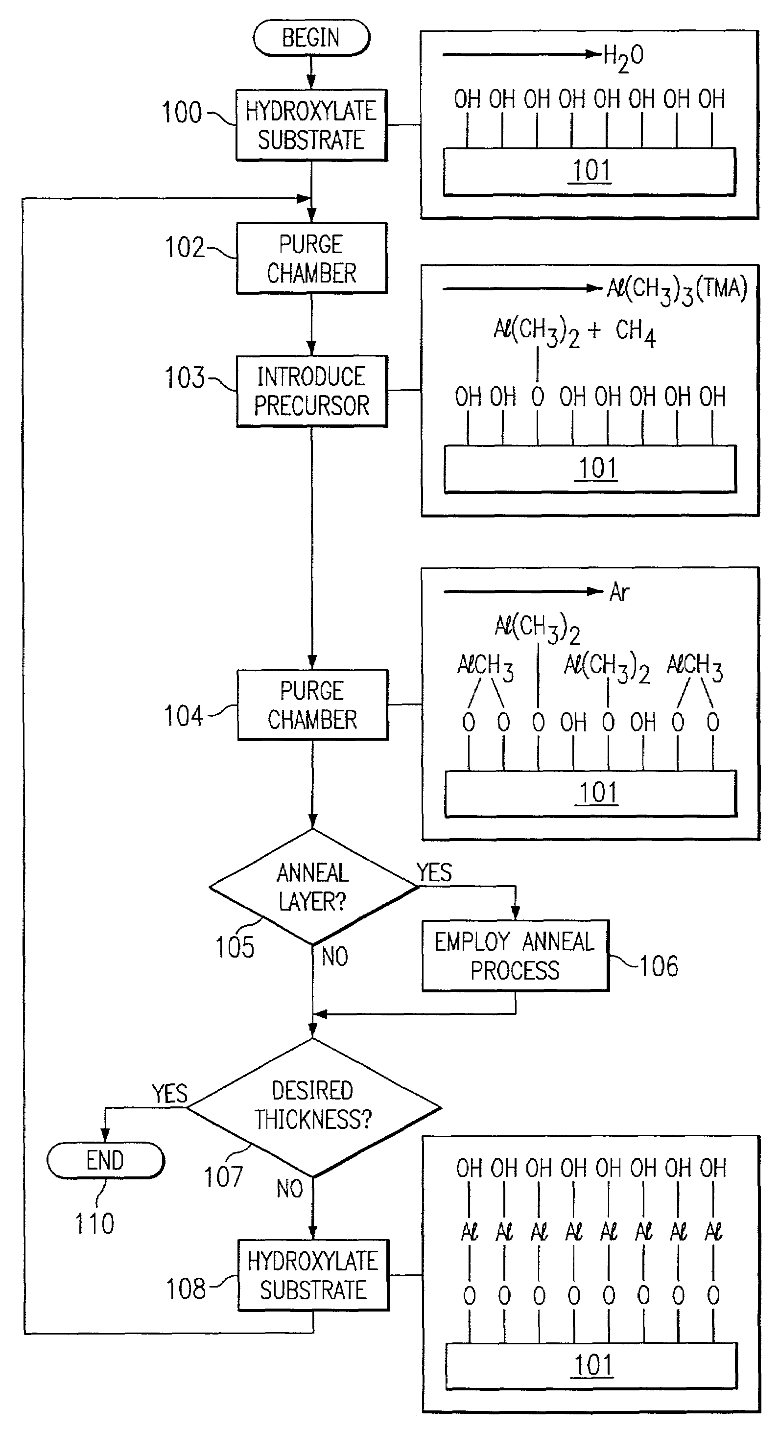
01 ALD process parameters for grain size control
Atomic layer deposition process parameters such as temperature, pressure, precursor flow rates, and cycle timing can be optimized to control the grain size of deposited thin films. The nucleation and growth mechanisms during ALD are highly dependent on these process conditions, which directly influence the final microstructure and grain boundaries of the deposited material.- ALD process parameters for grain size control: Atomic layer deposition process parameters such as temperature, pressure, precursor flow rates, and cycle timing can be optimized to control the grain size of deposited thin films. The nucleation and growth mechanisms during ALD cycles directly influence the final grain structure and crystallinity of the deposited material.
- Substrate surface treatment and nucleation enhancement: Surface preparation and nucleation layer techniques are employed to influence grain formation during atomic layer deposition. Surface treatments can provide controlled nucleation sites that affect the initial growth and subsequent grain development in thin films, leading to desired grain size distributions.
- Post-deposition annealing for grain size modification: Thermal annealing treatments after atomic layer deposition can significantly alter the grain structure of thin films. Heat treatment processes promote grain growth, recrystallization, and phase transformations that modify the microstructure and grain size characteristics of the deposited layers.
- Precursor chemistry effects on grain formation: The selection of specific precursor materials and their chemical properties influence the nucleation density and grain growth during atomic layer deposition. Different precursor combinations and reaction mechanisms can result in varying grain sizes and morphologies in the final thin film structure.
- Multi-layer and composite structures for grain engineering: Engineered multi-layer structures and composite thin films created through atomic layer deposition can be designed to achieve specific grain size characteristics. Layer thickness, composition gradients, and interface engineering techniques enable precise control over grain boundaries and overall microstructure.
02 Substrate surface treatment and nucleation control
Surface preparation and nucleation layer formation play critical roles in determining the initial grain formation during atomic layer deposition. Surface treatments, cleaning procedures, and nucleation enhancement techniques can significantly affect the density of nucleation sites and subsequent grain growth patterns in the deposited thin films.Expand Specific Solutions03 Post-deposition annealing and crystallization
Thermal treatment processes following atomic layer deposition can modify the grain structure and size of thin films. Annealing conditions including temperature profiles, atmosphere control, and duration affect grain growth, recrystallization, and phase transformations that ultimately determine the final grain size distribution.Expand Specific Solutions04 Material composition and precursor selection
The choice of precursor materials and their chemical properties influence the grain formation characteristics during atomic layer deposition. Different precursor combinations, dopant incorporation, and material compositions result in varying nucleation behaviors and grain growth kinetics, affecting the final microstructural properties of the deposited films.Expand Specific Solutions05 Film thickness and multilayer effects on grain structure
The relationship between film thickness and grain size evolution during atomic layer deposition involves complex growth mechanisms. Multilayer structures, interface effects, and thickness-dependent stress can influence grain coalescence, preferred orientation, and overall microstructural development throughout the deposition process.Expand Specific Solutions
Key Players in ALD Equipment and Thin Film Industry
The atomic layer deposition (ALD) thin film technology market is experiencing rapid growth, driven by increasing demand for precise nanoscale manufacturing in semiconductors and advanced materials. The industry is in a mature development stage with established players like Applied Materials, Picosun, and emerging competitors from Asia including Beijing NAURA and SK Hynix. Technology maturity varies significantly across the competitive landscape - while industry leaders like Applied Materials and Micron Technology demonstrate advanced ALD capabilities for high-volume production, specialized companies such as Picosun focus on innovative reactor designs. Research institutions including ETH Zurich, KIST, and Huazhong University of Science & Technology are driving fundamental breakthroughs in grain size control mechanisms. The market shows strong consolidation trends with major semiconductor manufacturers integrating ALD solutions, while equipment suppliers and material companies like Merck Patent GmbH compete for specialized applications in next-generation device manufacturing.
Applied Materials, Inc.
Technical Solution: Applied Materials develops advanced ALD systems with precise control over grain size through optimized precursor delivery and substrate temperature management. Their Endura platform integrates multiple ALD chambers with real-time monitoring capabilities to achieve uniform thin film deposition. The company's proprietary pulse timing algorithms and chamber design enable control of nucleation density, directly influencing grain size distribution. Their systems utilize advanced plasma-enhanced ALD (PEALD) technology to achieve lower deposition temperatures while maintaining film quality. The integration of in-situ metrology allows for real-time grain size monitoring and process adjustment during deposition.
Strengths: Industry-leading equipment with proven scalability and reliability for high-volume manufacturing. Weaknesses: High capital costs and complex system integration requirements.
Micron Technology, Inc.
Technical Solution: Micron Technology focuses on ALD process optimization for memory device applications, specifically targeting grain size control in high-k dielectrics and metal electrodes. Their approach involves systematic study of precursor chemistry effects on nucleation behavior and grain growth kinetics. The company develops specialized precursor formulations and deposition sequences to achieve desired grain structures for enhanced electrical properties. Their research emphasizes the correlation between ALD cycle parameters, substrate surface preparation, and resulting grain morphology. Micron's process development includes advanced characterization techniques to map grain size distribution across wafer surfaces and optimize uniformity for memory cell performance.
Strengths: Deep expertise in memory applications with strong process-property correlation understanding. Weaknesses: Limited focus outside memory applications, requiring adaptation for broader markets.
Core Innovations in ALD Grain Size Characterization
Atomic layer deposition device and method for preparing atomic layer deposition thin film
PatentWO2023178650A1
Innovation
- By forming a variable electric field in the reaction chamber of the atomic layer deposition equipment, the electric field is used to induce the polarity deflection and adsorption of the gas phase precursor, control the growth orientation of the film, and improve the deposition rate and quality.


Atomic layer deposition for fabricating thin films
PatentInactiveUS7037574B2
Innovation
- Implementing periodic annealing during ALD cycles with a dual zone showerhead to control precursor and reactant flow, purge cycles, and temperature, reducing impurity incorporation and enhancing throughput by varying the frequency of plasma anneals to control intrinsic stress and breakdown voltage.

Material Safety Standards for ALD Precursors
The safety of atomic layer deposition (ALD) precursors represents a critical aspect of thin film manufacturing processes, particularly when analyzing grain size influence requires extensive material handling and exposure protocols. Current material safety standards for ALD precursors are governed by multiple regulatory frameworks, including OSHA guidelines, EPA regulations, and international standards such as ISO 14040 series for environmental management.
Precursor materials used in ALD processes often contain highly reactive organometallic compounds, metal halides, and volatile organic substances that pose significant health and environmental risks. These materials typically exhibit characteristics such as pyrophoric behavior, corrosive properties, and potential carcinogenic effects. The establishment of comprehensive safety standards becomes particularly crucial when conducting grain size analysis studies, which may require prolonged exposure periods and repeated experimental cycles.
Primary safety protocols encompass proper storage conditions, including inert atmosphere requirements, temperature control systems, and segregation procedures to prevent incompatible material interactions. Handling procedures mandate the use of specialized personal protective equipment, including supplied-air respirators, chemical-resistant gloves, and full-body protection suits. Laboratory infrastructure must incorporate advanced ventilation systems, emergency shower facilities, and automated gas detection networks.
Waste management standards for ALD precursors follow strict classification systems based on hazard categories and disposal methods. Spent precursor materials and contaminated equipment require specialized treatment protocols, often involving neutralization processes or high-temperature incineration under controlled conditions. Documentation requirements include detailed material safety data sheets, exposure monitoring records, and incident reporting procedures.
Emerging safety standards address novel precursor chemistries and their potential long-term effects on human health and environmental systems. Recent developments focus on establishing exposure limits for newly synthesized organometallic compounds and implementing real-time monitoring systems for trace contamination detection. These evolving standards directly impact grain size analysis methodologies by influencing experimental design parameters and safety margin requirements.
Training and certification requirements for personnel handling ALD precursors continue to expand, incorporating specialized modules on emergency response procedures, chemical compatibility assessment, and environmental impact evaluation. Regular safety audits and compliance verification processes ensure adherence to established standards while promoting continuous improvement in safety protocols and risk mitigation strategies.
Quality Control Methods for ALD Grain Analysis
Quality control in ALD grain analysis requires sophisticated measurement techniques and standardized protocols to ensure accurate characterization of thin film microstructures. The primary challenge lies in establishing reliable methodologies that can consistently detect and quantify grain size variations across different substrate materials and deposition conditions.
X-ray diffraction (XRD) serves as the cornerstone technique for grain size analysis in ALD films. The Scherrer equation provides quantitative grain size measurements through peak broadening analysis, while Williamson-Hall plots help distinguish between size-induced and strain-induced broadening effects. Advanced XRD techniques such as grazing incidence diffraction enable surface-sensitive measurements crucial for ultrathin ALD layers.
Transmission electron microscopy (TEM) offers direct visualization of grain boundaries and crystalline structures at nanoscale resolution. Cross-sectional TEM imaging provides detailed information about grain morphology, orientation relationships, and interface characteristics. However, sample preparation artifacts and electron beam damage can introduce measurement uncertainties that require careful consideration in quality control protocols.
Atomic force microscopy (AFM) complements other techniques by providing surface topography information that correlates with underlying grain structures. Statistical analysis of AFM height distributions and grain boundary mapping enables quantitative assessment of surface roughness parameters directly related to grain size variations.
Standardization of measurement protocols is essential for reproducible results across different laboratories and equipment configurations. This includes establishing reference standards, calibration procedures, and data analysis methodologies. Sample preparation protocols must be optimized to minimize artifacts while preserving the native grain structure of ALD films.
Statistical process control methods integrate multiple measurement techniques to establish control limits and detect process variations. Real-time monitoring capabilities enable immediate feedback for process optimization, while long-term trending analysis identifies systematic changes in grain size distributions that may indicate equipment drift or process degradation.
Unlock deeper insights with PatSnap Eureka Quick Research — get a full tech report to explore trends and direct your research. Try now!
Generate Your Research Report Instantly with AI Agent
Supercharge your innovation with PatSnap Eureka AI Agent Platform!