How To Quantify Conformality Levels In Atomic Layer Deposition Applications
MAY 13, 20269 MIN READ
Generate Your Research Report Instantly with AI Agent
PatSnap Eureka helps you evaluate technical feasibility & market potential.
ALD Conformality Background and Quantification Goals
Atomic Layer Deposition has emerged as a critical thin film deposition technique in semiconductor manufacturing, particularly for advanced node technologies where precise thickness control and exceptional conformality are paramount. The technique's self-limiting surface reactions enable atomic-scale precision in film growth, making it indispensable for fabricating three-dimensional nanostructures, high-aspect-ratio features, and complex device architectures in modern electronics.
The fundamental principle of ALD relies on sequential, self-saturating surface reactions that theoretically provide perfect step coverage on all exposed surfaces. However, in practical applications, conformality levels vary significantly depending on process parameters, precursor chemistry, substrate geometry, and reactor design. This variability has created an urgent need for standardized quantification methods to ensure process reliability and product quality across different manufacturing environments.
Traditional conformality assessment methods have relied primarily on cross-sectional microscopy techniques, which provide qualitative visual information but lack the precision and standardization required for advanced manufacturing processes. These approaches often suffer from sampling limitations, measurement subjectivity, and inability to capture conformality variations across entire wafer surfaces or within complex three-dimensional structures.
The semiconductor industry's transition toward more complex device architectures, including FinFETs, gate-all-around transistors, and three-dimensional memory structures, has intensified the demand for quantitative conformality metrics. These advanced devices require conformal coatings with thickness uniformity exceeding 95% even in high-aspect-ratio trenches and via structures, necessitating precise measurement and control capabilities.
Current quantification challenges encompass multiple technical dimensions, including the development of non-destructive measurement techniques, establishment of industry-standard conformality metrics, and creation of predictive models that correlate process parameters with conformality outcomes. The lack of universally accepted quantification standards has hindered process optimization efforts and complicated technology transfer between different manufacturing facilities.
The primary goal of conformality quantification research focuses on developing robust, reproducible measurement methodologies that can accurately assess film thickness uniformity across complex topographies. These methodologies must accommodate various substrate geometries, from simple planar surfaces to intricate three-dimensional nanostructures, while providing statistically meaningful data for process control and optimization.
Secondary objectives include establishing correlations between conformality metrics and device performance parameters, enabling predictive process modeling, and developing real-time monitoring capabilities for production environments. Success in these areas would significantly enhance ALD process control capabilities and accelerate the development of next-generation semiconductor devices requiring exceptional conformality performance.
Market Demand for High-Conformality ALD Applications
The semiconductor industry represents the largest and most demanding market segment for high-conformality ALD applications. Advanced logic devices at nodes below 7nm require exceptional step coverage for gate dielectrics, where conformality directly impacts device performance and yield. Memory manufacturers, particularly in 3D NAND and DRAM production, face increasingly stringent conformality requirements as aspect ratios exceed 100:1 in vertical structures. The transition to extreme ultraviolet lithography and gate-all-around transistor architectures has intensified the need for precise conformality quantification methods.
Display technology markets, including OLED and micro-LED manufacturing, demand uniform thin film deposition across large substrate areas with complex topographies. Flexible display applications require ALD processes that maintain conformality during mechanical stress, driving demand for real-time conformality monitoring systems. The automotive display segment particularly emphasizes reliability standards that necessitate comprehensive conformality validation protocols.
Power semiconductor applications in electric vehicles and renewable energy systems require robust ALD barrier layers with verified conformality performance. Wide bandgap semiconductors like silicon carbide and gallium nitride present unique conformality challenges due to their crystalline structures and processing temperatures. These applications often operate in harsh environments where conformality defects can lead to catastrophic failures.
The photovoltaics industry increasingly adopts ALD for passivation layers and transparent conductive oxides, where conformality directly correlates with energy conversion efficiency. Perovskite solar cells and tandem architectures require precise conformality control to optimize optical and electrical properties across textured surfaces.
Emerging quantum computing and neuromorphic device markets represent high-value applications where atomic-scale conformality control becomes critical. These technologies require novel quantification approaches that can detect sub-nanometer variations in film thickness and composition uniformity.
Medical device manufacturing, particularly for implantable electronics and biosensors, demands biocompatible ALD coatings with verified conformality to ensure long-term stability and performance. Regulatory requirements in this sector drive the need for standardized conformality measurement protocols and traceability systems.
The growing complexity of these applications creates substantial market pressure for advanced conformality quantification tools that can provide real-time feedback, statistical process control capabilities, and integration with existing manufacturing execution systems.
Current ALD Conformality Measurement Challenges
The quantification of conformality in atomic layer deposition processes faces significant measurement challenges that stem from both technical limitations and standardization gaps. Traditional characterization methods often fall short in providing comprehensive conformality assessment across diverse substrate geometries and feature scales.
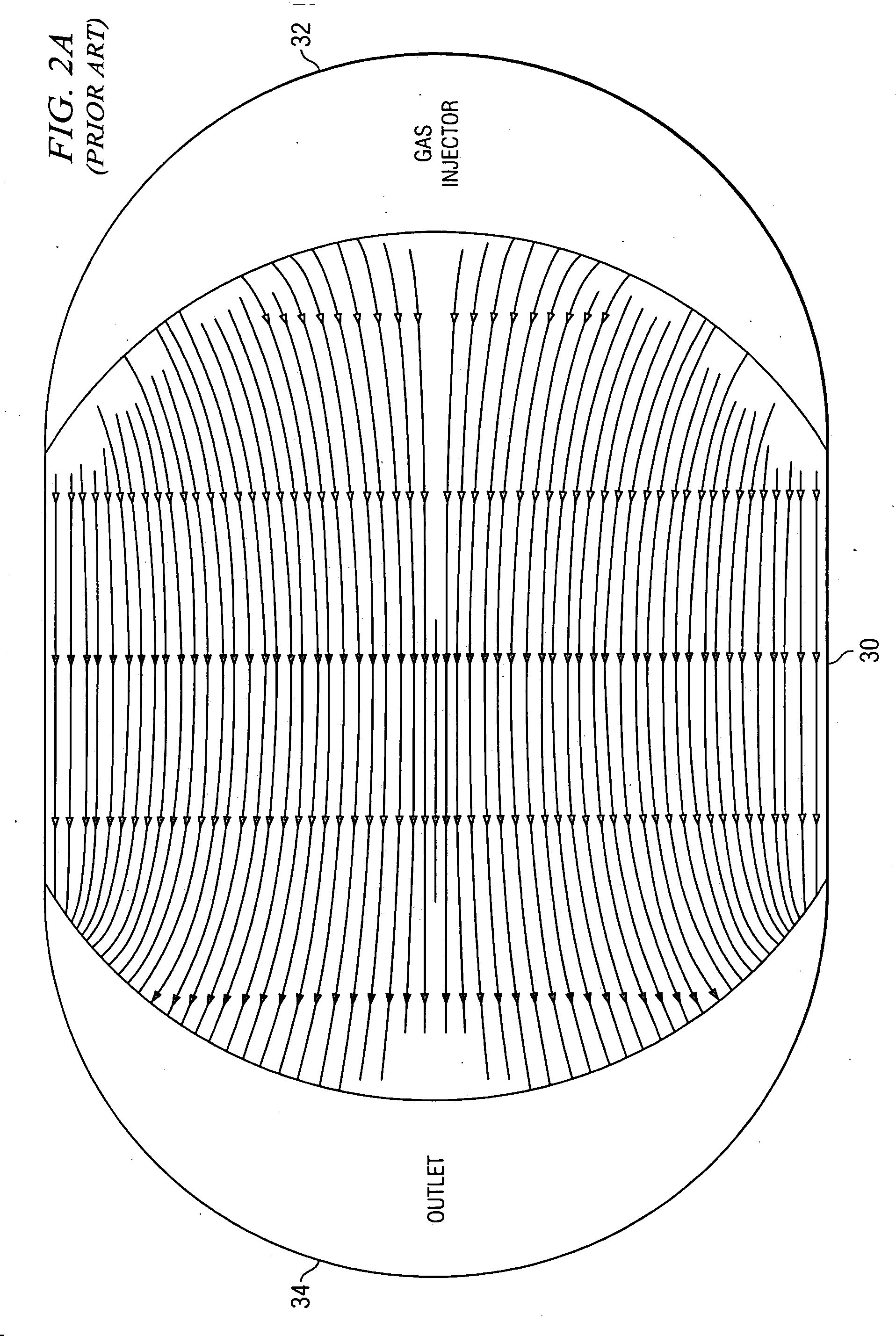
Cross-sectional scanning electron microscopy remains the most widely adopted technique for conformality evaluation, yet it suffers from inherent limitations including destructive sample preparation, limited statistical sampling, and potential artifacts introduced during specimen processing. The method provides only localized information and cannot capture conformality variations across entire wafer surfaces or within complex three-dimensional structures.
Ellipsometry-based measurements, while non-destructive, face substantial challenges when applied to high-aspect-ratio features and complex topographies. The technique struggles with accurate thickness determination in trenches and vias where optical access is restricted, leading to significant measurement uncertainties. Additionally, the assumption of uniform optical properties across conformal films may not hold for ALD processes operating under non-ideal conditions.
The lack of standardized conformality metrics presents another critical challenge. Current industry practices rely on various definitions including step coverage ratios, thickness uniformity indices, and geometric conformality factors, making cross-platform comparisons and process benchmarking extremely difficult. This inconsistency hampers technology transfer and process optimization efforts across different manufacturing environments.
Real-time monitoring capabilities remain severely limited, with most conformality assessments conducted post-deposition. This approach prevents in-situ process adjustments and limits the ability to detect conformality degradation during extended deposition cycles. The absence of reliable real-time feedback mechanisms significantly impacts process control and yield optimization.
Furthermore, the measurement of conformality in emerging applications such as flexible electronics, MEMS devices, and advanced packaging structures introduces additional complexities. These applications often involve non-planar substrates, temperature-sensitive materials, and unconventional geometries that challenge existing measurement paradigms and require novel characterization approaches.
Existing Conformality Quantification Techniques
01 ALD process parameter optimization for conformality
Atomic layer deposition conformality can be enhanced through precise control of process parameters including temperature, pressure, precursor pulse timing, and purge cycles. Optimizing these parameters ensures uniform film thickness across complex three-dimensional structures and high aspect ratio features. The sequential nature of precursor exposure and reaction cycles allows for better step coverage compared to conventional deposition methods.- ALD process optimization for enhanced conformality: Atomic layer deposition processes can be optimized through precise control of reaction parameters, temperature cycling, and precursor delivery methods to achieve superior conformal coating on complex three-dimensional structures. Advanced process control techniques enable uniform film thickness distribution across high aspect ratio features and intricate geometries.
- Precursor chemistry and reaction mechanisms for conformal deposition: The selection and design of appropriate precursor materials and their reaction pathways significantly influence the conformality of deposited films. Optimized precursor chemistry ensures complete surface reactions and uniform coverage, particularly in challenging substrate topographies with narrow trenches and high aspect ratios.
- Substrate surface preparation and treatment methods: Surface conditioning and preparation techniques play a crucial role in achieving optimal conformality levels during atomic layer deposition. Proper substrate treatment ensures uniform nucleation sites and promotes consistent film growth across varying surface features and materials.
- Equipment design and reactor configuration for improved conformality: Specialized reactor designs and equipment configurations are developed to enhance gas flow distribution and precursor exposure uniformity. Advanced chamber geometries and gas delivery systems ensure consistent precursor access to all substrate surfaces, improving overall conformality performance.
- Measurement and characterization techniques for conformality assessment: Various analytical methods and measurement techniques are employed to evaluate and quantify conformality levels in atomic layer deposited films. These characterization approaches enable precise assessment of film thickness uniformity and coverage quality across complex substrate geometries.
02 Precursor chemistry and reaction mechanisms
The selection of appropriate precursor materials and understanding their surface reaction mechanisms is crucial for achieving high conformality levels. Different precursor combinations exhibit varying degrees of surface saturation and reaction kinetics, directly impacting the uniformity of film deposition. Self-limiting surface reactions ensure consistent layer-by-layer growth across substrate topography.Expand Specific Solutions03 Substrate surface preparation and treatment
Surface conditioning and preparation techniques significantly influence conformality performance in atomic layer deposition processes. Proper substrate cleaning, surface activation, and nucleation layer formation create optimal conditions for uniform film growth. Surface chemistry modifications can enhance precursor adsorption and improve step coverage on challenging geometries.Expand Specific Solutions04 Equipment design and reactor configuration
Reactor chamber design, gas flow dynamics, and precursor delivery systems play critical roles in achieving uniform conformality across substrate surfaces. Advanced reactor configurations with optimized gas distribution and temperature control enable better precursor transport into high aspect ratio structures. Specialized equipment features support consistent deposition conditions throughout the process cycle.Expand Specific Solutions05 Measurement and characterization methods
Various analytical techniques and measurement methods are employed to evaluate and quantify conformality levels in atomic layer deposited films. These characterization approaches include cross-sectional analysis, thickness mapping, and surface profiling to assess uniformity across different substrate features. Advanced metrology tools enable precise monitoring of deposition quality and process optimization.Expand Specific Solutions
Key Players in ALD Equipment and Metrology Industry
The atomic layer deposition (ALD) conformality quantification field represents a mature technology sector experiencing significant growth driven by advanced semiconductor manufacturing demands. The market demonstrates substantial scale with established equipment manufacturers like Applied Materials, Lam Research, and Samsung Electronics leading traditional ALD applications, while specialized companies such as NEXUSBE and ASM IP Holding focus on next-generation conformality solutions. Technology maturity varies across segments, with companies like Intel, Micron Technology, and LG Chem driving high-volume production applications, while research institutions including Imec and Ghent University advance fundamental conformality measurement techniques. The competitive landscape shows consolidation around precision metrology capabilities, with LayTec and Agilent Technologies providing specialized measurement solutions, and emerging players like VitriVax exploring novel applications beyond traditional semiconductor manufacturing.
Applied Materials, Inc.
Technical Solution: Applied Materials has developed advanced in-situ metrology solutions for ALD conformality quantification, including real-time ellipsometry and reflectometry systems integrated directly into ALD chambers. Their approach combines optical measurement techniques with machine learning algorithms to analyze film thickness uniformity across complex 3D structures. The company's SEMVision system provides cross-sectional analysis capabilities for post-deposition conformality assessment, while their process control software enables real-time monitoring and adjustment of deposition parameters to optimize conformality. Their solutions can quantify conformality levels with sub-nanometer precision across various substrate geometries including high aspect ratio trenches and via structures.
Strengths: Industry-leading equipment integration, comprehensive metrology portfolio, strong R&D capabilities. Weaknesses: High equipment costs, complex system integration requirements.
Samsung Electronics Co., Ltd.
Technical Solution: Samsung has developed proprietary conformality measurement methodologies specifically for advanced semiconductor manufacturing, focusing on 3D NAND and DRAM applications. Their approach utilizes a combination of transmission electron microscopy (TEM) analysis and electrical testing methods to quantify ALD conformality in high aspect ratio structures. The company has established standardized protocols for measuring step coverage percentages and thickness uniformity across different feature sizes, ranging from sub-10nm to several micrometers. Samsung's methodology includes statistical analysis frameworks for correlating conformality metrics with device performance parameters, enabling process optimization for next-generation memory devices.
Strengths: Deep semiconductor manufacturing expertise, advanced characterization capabilities, strong process integration knowledge. Weaknesses: Limited commercial availability of methodologies, focus primarily on memory applications.
Core Innovations in ALD Conformality Measurement
Method for improved processing with neutral radicals and other mean free path limited species
PatentInactiveUS20210262088A1
Innovation
- The method involves using mean free path limited species such as neutral atomic species, neutral molecular radicals, and electrons, which are generated and delivered directionally to the substrate, often with the assistance of inert gases to improve conformality and mitigate 'RF damage' by operating in the Knudsen or molecular flow regimes, ensuring a gentle deposition process.


Method and apparatus for fabricating a conformal thin film on a substrate
PatentInactiveUS20050100669A1
Innovation
- A diffuser plate with a protrusion is used in the ALD system to reduce turbulence in the expansion volume, facilitating laminar gas flow and uniform precursor distribution, thereby improving the efficiency of the purge process and reducing gas phase reactions.

Standardization Efforts for ALD Conformality Metrics
The standardization of ALD conformality metrics has emerged as a critical priority within the semiconductor industry, driven by the increasing complexity of three-dimensional device architectures and the need for reproducible measurement protocols. Currently, multiple organizations are actively working to establish unified standards that can be adopted across different manufacturing environments and research institutions.
The International Technology Roadmap for Semiconductors (ITRS) and its successor, the International Roadmap for Devices and Systems (IRDS), have identified conformality quantification as a key metrology challenge requiring immediate attention. These roadmaps emphasize the necessity for standardized definitions of conformality parameters, including step coverage ratios, thickness uniformity indices, and aspect ratio-dependent deposition rates.
SEMI, the global industry association serving the manufacturing supply chains for the microelectronic, display, and photovoltaic industries, has initiated working groups specifically focused on ALD conformality standards. These groups are developing comprehensive guidelines for measurement methodologies, sample preparation protocols, and data reporting formats. The proposed standards aim to establish consistent terminology and calculation methods that can be universally applied across different ALD systems and applications.
The American Society for Testing and Materials (ASTM) has also contributed significantly to this standardization effort through its Committee F01 on Electronics, which has been developing test methods for evaluating thin film conformality in high aspect ratio structures. These standards focus on cross-sectional analysis techniques, statistical sampling requirements, and uncertainty quantification methods.
International collaboration has been facilitated through the International Electrotechnical Commission (IEC), which is working to harmonize regional standards and ensure global compatibility. The IEC's technical committees are addressing the challenges of correlating different measurement techniques and establishing traceability chains for conformality measurements.
Recent progress includes the development of reference materials and certified test structures that enable interlaboratory comparisons and method validation. These standardization efforts are expected to accelerate the adoption of quantitative conformality assessment in industrial ALD processes, ultimately improving process control and yield optimization across the semiconductor manufacturing ecosystem.
Process Control Integration for Real-Time Conformality
The integration of process control systems for real-time conformality monitoring represents a critical advancement in atomic layer deposition technology. Modern ALD systems require sophisticated control architectures that can simultaneously manage multiple process parameters while continuously assessing film conformality across complex three-dimensional structures. This integration involves the deployment of advanced sensor networks, real-time data processing capabilities, and automated feedback mechanisms that work in concert to maintain optimal deposition conditions.
Real-time conformality assessment relies on the seamless integration of multiple measurement techniques within the process control framework. In-situ ellipsometry, optical emission spectroscopy, and mass spectrometry data streams must be synchronized and processed through advanced algorithms that can interpret conformality indicators in real-time. The control system architecture typically employs distributed processing nodes that handle specific measurement modalities while communicating through high-speed data buses to ensure minimal latency in conformality assessment.
The implementation of closed-loop control for conformality optimization requires sophisticated process models that correlate measurable parameters with conformality outcomes. These models incorporate machine learning algorithms trained on extensive datasets linking process conditions such as precursor pulse timing, purge durations, substrate temperature profiles, and reactor pressure dynamics to conformality metrics. The control system continuously updates these models based on real-time measurements, enabling adaptive process optimization.
Advanced process control integration also encompasses predictive maintenance capabilities that monitor system components affecting conformality performance. Precursor delivery system health, reactor chamber condition, and substrate handling mechanisms are continuously evaluated to prevent conformality degradation due to equipment drift or component wear. This holistic approach ensures consistent conformality performance across extended production runs.
The scalability of integrated control systems presents unique challenges for high-volume manufacturing environments. Multi-chamber systems require coordinated control strategies that maintain conformality consistency across parallel processing units while optimizing overall throughput. Load balancing algorithms distribute substrates based on real-time conformality performance metrics from individual chambers, ensuring uniform product quality across the entire production system.
Unlock deeper insights with PatSnap Eureka Quick Research — get a full tech report to explore trends and direct your research. Try now!
Generate Your Research Report Instantly with AI Agent
Supercharge your innovation with PatSnap Eureka AI Agent Platform!