Compare Single And Multilayer Atomic Layer Deposition Films For Adhesion
MAY 13, 20269 MIN READ
Generate Your Research Report Instantly with AI Agent
PatSnap Eureka helps you evaluate technical feasibility & market potential.
ALD Film Adhesion Technology Background and Objectives
Atomic Layer Deposition (ALD) has emerged as a critical thin film deposition technique since its development in the 1970s, revolutionizing the semiconductor industry and expanding into diverse applications including energy storage, catalysis, and protective coatings. The technology's unique self-limiting surface reactions enable precise control over film thickness at the atomic level, making it indispensable for modern nanoscale device fabrication where traditional deposition methods fall short.
The evolution of ALD technology has progressed from simple binary oxide films to complex multilayer architectures, driven by the increasing demand for enhanced material properties and device performance. Early ALD applications focused primarily on achieving uniform, conformal coatings on high-aspect-ratio structures. However, as device dimensions continued to shrink and performance requirements intensified, the limitations of single-layer ALD films became apparent, particularly regarding adhesion properties and interfacial stability.
Film adhesion represents one of the most critical challenges in ALD applications, directly impacting device reliability, mechanical stability, and long-term performance. Poor adhesion can lead to delamination, interfacial failure, and catastrophic device malfunction, making it a paramount concern for manufacturers across industries. The adhesion quality depends on multiple factors including substrate surface preparation, interfacial chemistry, film stress, and thermal expansion mismatch.
The primary objective of comparing single and multilayer ALD films for adhesion is to establish a comprehensive understanding of how layer architecture influences interfacial bonding mechanisms and overall film stability. Single-layer films offer simplicity in processing and characterization but may suffer from limited adhesion optimization opportunities. Conversely, multilayer structures provide additional degrees of freedom through engineered interfaces, gradient compositions, and stress management layers.
This technological investigation aims to identify optimal film architectures that maximize adhesion strength while maintaining desired functional properties. The research seeks to elucidate the fundamental mechanisms governing adhesion in both configurations, including the role of interfacial reactions, mechanical interlocking, and chemical bonding. Understanding these mechanisms will enable the development of design principles for next-generation ALD processes that can meet increasingly stringent adhesion requirements in advanced applications such as flexible electronics, automotive components, and aerospace systems.
Market Demand for Enhanced ALD Film Adhesion Solutions
The semiconductor industry represents the primary driving force behind enhanced ALD film adhesion solutions, with advanced node manufacturing requiring increasingly sophisticated thin film deposition techniques. As device geometries shrink below 7nm and approach 3nm technology nodes, the demand for superior adhesion properties becomes critical for maintaining device reliability and performance. The transition from planar to three-dimensional device architectures, including FinFET and gate-all-around structures, necessitates conformal coating with exceptional adhesion characteristics across complex topographies.
Memory device manufacturers constitute another significant market segment, particularly in the production of 3D NAND flash and next-generation storage technologies. The vertical stacking of memory cells requires multilayer ALD films with consistent adhesion properties throughout the entire structure. Poor adhesion can lead to delamination during subsequent processing steps, resulting in device failure and reduced manufacturing yields.
The emerging flexible electronics market presents substantial growth opportunities for enhanced ALD adhesion solutions. Flexible displays, wearable devices, and bendable sensors require thin films that maintain adhesion under mechanical stress and repeated flexing. Traditional single-layer ALD approaches often fail to meet these demanding requirements, creating market demand for innovative multilayer solutions that can accommodate substrate deformation while preserving electrical and optical properties.
Power electronics applications, including wide bandgap semiconductors and high-voltage devices, require ALD films with superior adhesion to withstand thermal cycling and mechanical stress. The automotive industry's shift toward electric vehicles and the growing renewable energy sector drive demand for more robust thin film solutions that can operate reliably under harsh environmental conditions.
The photovoltaic industry increasingly relies on ALD technology for surface passivation and anti-reflective coatings, where adhesion directly impacts long-term device performance and durability. Solar panel manufacturers seek solutions that maintain adhesion over decades of outdoor exposure while preserving optical and electrical properties.
Market growth is further accelerated by the Internet of Things expansion, requiring miniaturized sensors and electronic components with reliable thin film coatings. The proliferation of edge computing devices and autonomous systems creates additional demand for enhanced adhesion solutions that ensure long-term reliability in diverse operating environments.
Current ALD Adhesion Challenges and Global Development Status
Atomic Layer Deposition (ALD) technology faces significant adhesion challenges that vary substantially between single-layer and multilayer film configurations. The primary adhesion issues stem from interfacial stress accumulation, thermal expansion coefficient mismatches, and chemical bonding incompatibilities between deposited films and substrate materials. These challenges become increasingly complex in multilayer systems where interlayer adhesion must be maintained alongside substrate adhesion.
Current adhesion failures in ALD films manifest through several mechanisms including delamination at substrate interfaces, interlayer separation in multilayer stacks, and stress-induced cracking during thermal cycling. Single-layer ALD films typically exhibit adhesion challenges related to surface preparation quality, nucleation density variations, and inherent stress development during deposition. The adhesion strength is heavily dependent on substrate surface chemistry and the initial nucleation behavior of precursor molecules.
Multilayer ALD systems present additional complexity as each interface introduces potential failure points. Interlayer adhesion depends on chemical compatibility between adjacent materials, processing temperature sequences, and cumulative stress effects. The global development status reveals that multilayer adhesion challenges are particularly pronounced in applications requiring dissimilar materials such as oxide-metal-oxide stacks or alternating high-k and low-k dielectric layers.
Geographically, adhesion research leadership is concentrated in advanced semiconductor regions including Taiwan, South Korea, and specific clusters in the United States and Europe. Asian manufacturers focus primarily on high-volume production challenges, while European and American research emphasizes fundamental adhesion mechanisms and novel material combinations. The development landscape shows varying priorities with Asian facilities addressing immediate manufacturing yield issues and Western research institutions exploring next-generation material systems.
Current measurement and characterization limitations significantly impact adhesion assessment capabilities. Standard adhesion testing methods often prove inadequate for ultra-thin ALD films, necessitating specialized techniques such as nanoindentation, scratch testing, and thermal stress analysis. The industry lacks standardized protocols for multilayer adhesion evaluation, creating inconsistencies in comparative studies and hindering systematic improvement efforts.
The economic impact of adhesion failures drives substantial research investment globally. Manufacturing yield losses due to delamination and adhesion-related defects represent significant cost factors in semiconductor and advanced coating industries. This economic pressure accelerates development of improved surface preparation techniques, interfacial engineering approaches, and stress management strategies across different geographical regions.
Current ALD Film Adhesion Enhancement Approaches
01 Surface treatment and preparation methods for enhanced adhesion
Various surface treatment techniques are employed to improve the adhesion of atomic layer deposition films to substrates. These methods include plasma treatment, chemical cleaning, and surface modification processes that create favorable bonding sites. The treatments help remove contaminants and create reactive surface groups that promote better film-substrate interaction and reduce delamination issues.- Surface treatment and preparation methods for enhanced adhesion: Various surface treatment techniques are employed to improve the adhesion of atomic layer deposition films to substrates. These methods include plasma treatment, chemical cleaning, and surface modification processes that create favorable bonding sites. The treatments help remove contaminants and create reactive surface groups that promote better film-substrate interaction and reduce delamination issues.
- Interfacial layer engineering and buffer layers: The implementation of interfacial layers and buffer layers between the substrate and the main film significantly improves adhesion properties. These intermediate layers serve as adhesion promoters by providing better lattice matching and reducing stress at the interface. The buffer layers can be composed of different materials that create a gradual transition in properties from the substrate to the deposited film.
- Temperature and process parameter optimization: Controlling deposition temperature, pressure, and precursor flow rates during the atomic layer deposition process is crucial for achieving optimal film adhesion. Lower temperatures may be used to reduce thermal stress, while specific temperature profiles can promote better nucleation and growth. Process parameters are carefully tuned to minimize film stress and maximize interfacial bonding strength.
- Chemical bonding enhancement and precursor selection: The choice of precursor materials and their chemical properties directly affects the adhesion quality of deposited films. Specific precursors that form strong chemical bonds with the substrate surface are selected to improve adhesion. The precursor chemistry influences the nucleation behavior and the formation of interfacial bonds, leading to better film stability and reduced peeling or cracking.
- Stress management and film structure control: Managing internal stress within the deposited films is essential for maintaining good adhesion properties. Techniques include controlling film thickness, implementing stress-relief structures, and optimizing the crystalline structure of the deposited material. Proper stress management prevents film cracking and delamination while maintaining the desired electrical and mechanical properties of the final device structure.
02 Interfacial layer engineering and buffer layers
The implementation of interfacial layers or buffer layers between the substrate and the main film significantly improves adhesion properties. These intermediate layers are designed to provide better lattice matching, reduce stress, and create stronger chemical bonds. The buffer layers can be composed of different materials that act as adhesion promoters and help accommodate thermal expansion differences.Expand Specific Solutions03 Temperature and process parameter optimization
Controlling deposition temperature, pressure, and precursor flow rates during the atomic layer deposition process is crucial for achieving optimal film adhesion. Lower temperatures may be used to reduce thermal stress, while specific temperature profiles can promote better nucleation and growth. Process parameters are carefully tuned to minimize film stress and maximize interfacial bonding strength.Expand Specific Solutions04 Chemical bonding enhancement and precursor selection
The choice of precursor materials and their chemical properties directly affects the adhesion quality of deposited films. Specific precursors are selected based on their ability to form strong chemical bonds with the substrate surface. Reactive precursors that can create covalent bonds or form intermediate compounds at the interface are preferred to improve overall film adhesion and durability.Expand Specific Solutions05 Post-deposition treatments and annealing processes
Various post-deposition treatments including thermal annealing, plasma exposure, and chemical treatments are applied to enhance film adhesion after the initial deposition. These treatments help relieve internal stress, promote interdiffusion at interfaces, and strengthen chemical bonds. Controlled annealing processes can also improve crystallinity and reduce defects that may compromise adhesion.Expand Specific Solutions
Major ALD Equipment and Materials Industry Players
The atomic layer deposition (ALD) adhesion technology sector represents a mature yet rapidly evolving market within the broader semiconductor manufacturing industry. The competitive landscape spans established semiconductor equipment giants like Tokyo Electron, ASM International, and Samsung Electronics, alongside specialized ALD providers such as Picosun and SUPERALD. Major foundries including SMIC-Beijing and memory manufacturers like Micron Technology drive significant demand for both single and multilayer ALD solutions. The technology has reached commercial maturity with proven applications in semiconductor device fabrication, though innovation continues in multilayer architectures for enhanced adhesion properties. Research institutions like Huazhong University of Science & Technology and Fudan University contribute fundamental research, while industrial players focus on scaling production capabilities. The market demonstrates strong growth potential driven by advanced node requirements and emerging applications in flexible electronics and energy storage devices.
Tokyo Electron Ltd.
Technical Solution: Tokyo Electron's ALD technology emphasizes comparative analysis between single and multilayer film structures for enhanced adhesion performance. Their approach includes surface modification techniques, optimized precursor chemistry, and temperature-controlled deposition processes. The company develops specialized recipes for multilayer ALD films that incorporate adhesion-promoting interlayers and stress-relief mechanisms. Their systems enable precise thickness control and interface engineering to maximize adhesion strength across different material combinations in semiconductor manufacturing.
Strengths: Comprehensive process development capabilities and strong semiconductor industry presence. Weaknesses: Limited focus on non-semiconductor applications and high maintenance requirements.
International Business Machines Corp.
Technical Solution: IBM's research focuses on fundamental understanding of adhesion mechanisms in single versus multilayer ALD films through advanced characterization techniques. Their approach involves molecular-level interface analysis, stress engineering, and novel precursor development to optimize film adhesion. IBM investigates the role of interfacial chemistry, thermal expansion mismatch, and mechanical properties in determining adhesion performance. Their multilayer strategies include gradient compositions and buffer layers to enhance overall film-substrate adhesion in advanced microelectronics applications.
Strengths: Strong research capabilities and fundamental understanding of ALD mechanisms. Weaknesses: Limited commercial ALD equipment manufacturing and focus primarily on research applications.
Core Patents in Single vs Multilayer ALD Adhesion
Laminates and gas barrier films
PatentActiveUS20180036998A1
Innovation
- A laminate structure is proposed, comprising a substrate with an atomic layer deposition film coated with a protective film having an adhesive layer that provides sufficient adhesion to prevent damage while allowing easy peeling without causing harm to the underlying film, with specific adhesive force and thickness ranges to ensure optimal protection and handling.


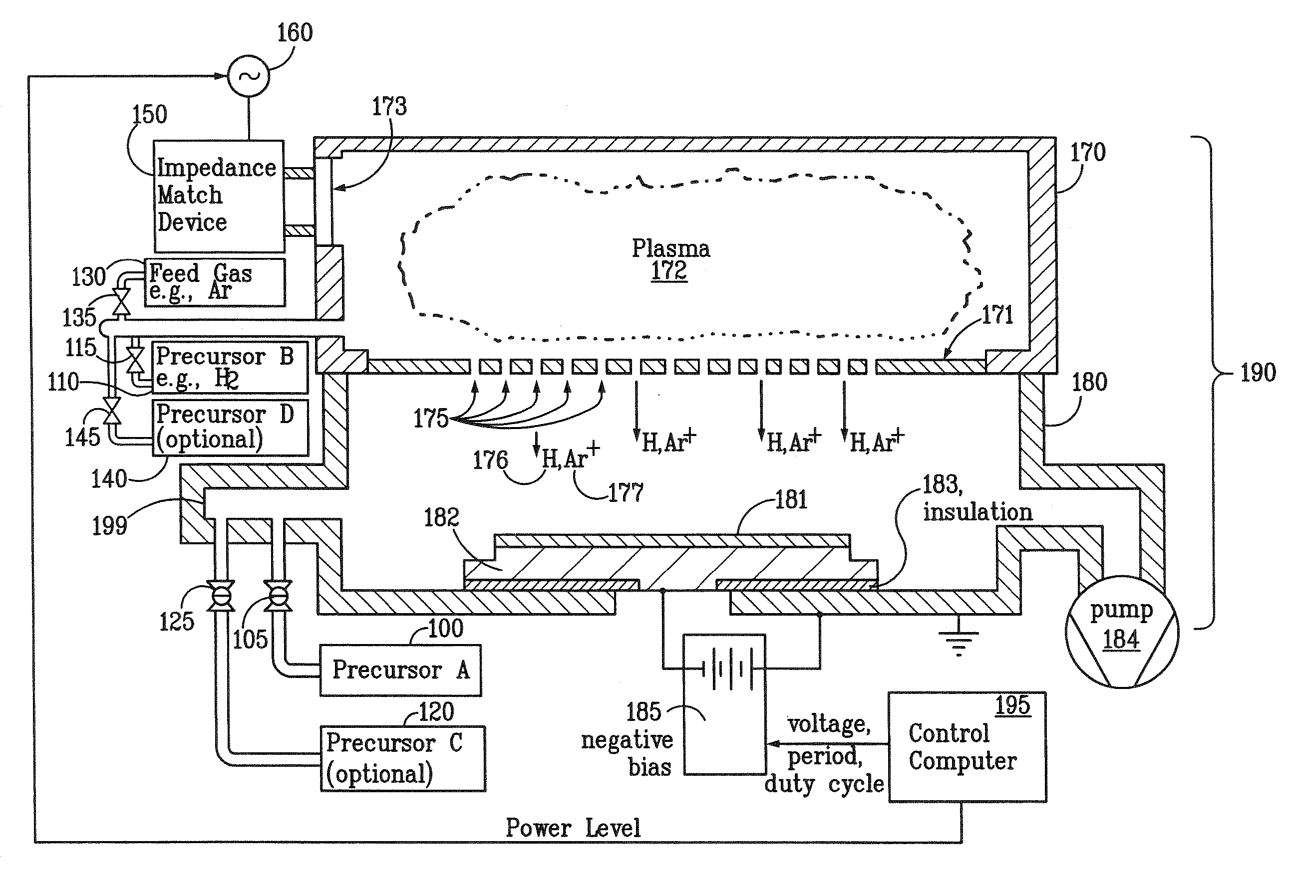
System for Depositing a Film by Modulated Ion-Induced Atomic Layer Deposition (MII-ALD)
PatentInactiveUS20110017139A1
Innovation
- The modulated ion-induced atomic layer deposition (MII-ALD) method uses ion bombardment as a non-thermal activation source to drive the deposition reaction, employing a microwave-generated plasma to generate ions and radicals efficiently, allowing for lower substrate temperatures and faster deposition rates, while maintaining high film purity and adhesion properties.
ALD Process Safety and Environmental Regulations
The implementation of atomic layer deposition processes for both single and multilayer film applications necessitates comprehensive adherence to stringent safety protocols and environmental regulations. ALD operations involve the use of highly reactive precursor chemicals, many of which pose significant health and environmental risks due to their toxic, corrosive, or pyrophoric nature. Common precursors such as trimethylaluminum, titanium tetrachloride, and various metal-organic compounds require specialized handling procedures to prevent exposure and environmental contamination.
Process safety considerations encompass multiple critical aspects including proper ventilation systems, emergency response protocols, and personnel protective equipment requirements. ALD reactors must be equipped with advanced exhaust systems capable of neutralizing toxic byproducts and unreacted precursors before atmospheric release. The high-temperature processing conditions typical in ALD operations demand robust thermal management systems and fail-safe mechanisms to prevent equipment malfunction and potential hazardous material release.
Environmental regulations governing ALD processes vary significantly across jurisdictions but generally focus on air quality standards, waste disposal requirements, and chemical inventory reporting. The Occupational Safety and Health Administration and Environmental Protection Agency in the United States, along with similar regulatory bodies globally, have established specific guidelines for semiconductor manufacturing processes that directly impact ALD operations. These regulations mandate continuous monitoring of workplace air quality, proper disposal of chemical waste streams, and maintenance of detailed chemical usage records.
Waste management protocols for ALD processes require careful consideration of both liquid and gaseous waste streams. Spent precursor materials and cleaning solvents must be classified and disposed of according to hazardous waste regulations, while exhaust gases require treatment through scrubbing systems or thermal oxidation units. The implementation of closed-loop systems and precursor recycling technologies has become increasingly important for regulatory compliance and cost reduction.
Recent regulatory developments have emphasized the importance of life cycle assessment approaches in evaluating the environmental impact of ALD processes. This includes consideration of precursor synthesis, transportation, usage efficiency, and end-of-life disposal impacts. Companies implementing ALD technologies must demonstrate compliance through comprehensive environmental management systems and regular third-party auditing processes to ensure continued regulatory adherence and operational sustainability.
ALD Film Quality Standards and Testing Methodologies
The establishment of comprehensive quality standards for ALD films represents a critical foundation for evaluating adhesion performance across single and multilayer configurations. Industry standards such as ASTM F1372 and ISO 14577 provide frameworks for mechanical property assessment, while specialized protocols address the unique characteristics of atomic layer deposited materials. These standards encompass film thickness uniformity, conformality, chemical composition, and interfacial properties that directly influence adhesion behavior.
Standardized testing methodologies for ALD film adhesion evaluation include both qualitative and quantitative approaches. The tape test method (ASTM D3359) offers rapid screening capabilities, while scratch testing (ASTM C1624) provides controlled mechanical stress application to determine critical loads for film delamination. Cross-cut adhesion testing enables systematic evaluation of coating-substrate bonding strength through standardized grid patterns and adhesive tape removal procedures.
Advanced characterization techniques complement traditional adhesion testing methods. Nanoindentation testing allows precise measurement of mechanical properties at the nanoscale, revealing differences between single and multilayer ALD structures. Pull-off testing using portable adhesion testers provides quantitative adhesion strength measurements in megapascals, enabling direct comparison between different film architectures and substrate combinations.
Interfacial analysis methodologies play crucial roles in understanding adhesion mechanisms. X-ray photoelectron spectroscopy (XPS) depth profiling reveals chemical bonding states and elemental distribution across film-substrate interfaces. Transmission electron microscopy (TEM) cross-sectional analysis provides atomic-scale visualization of interfacial structures, particularly valuable for multilayer systems where interlayer adhesion becomes critical.
Environmental testing protocols ensure adhesion performance under real-world conditions. Thermal cycling tests evaluate adhesion stability across temperature ranges, while humidity exposure assessments determine moisture sensitivity effects on film-substrate bonding. Salt spray testing and corrosion resistance evaluations provide insights into long-term adhesion performance in harsh environments.
Statistical analysis frameworks support reliable adhesion data interpretation. Multiple sample testing with appropriate statistical significance ensures reproducible results, while Weibull analysis helps characterize adhesion strength distributions and failure probability predictions for both single and multilayer ALD configurations.
Unlock deeper insights with PatSnap Eureka Quick Research — get a full tech report to explore trends and direct your research. Try now!
Generate Your Research Report Instantly with AI Agent
Supercharge your innovation with PatSnap Eureka AI Agent Platform!