

Analyzing Iron Oxide’s Impact on Semiconductor Performance
FEB 12, 20269 MIN READ
Generate Your Research Report Instantly with AI Agent
Patsnap Eureka helps you evaluate technical feasibility & market potential.
Iron Oxide Contamination Background and Objectives
Iron oxide contamination represents one of the most critical challenges in modern semiconductor manufacturing, where even trace amounts at parts-per-billion levels can severely compromise device performance and yield. As semiconductor technology nodes continue to shrink below 5 nanometers, the tolerance for metallic impurities has decreased exponentially, making iron oxide contamination a paramount concern for the industry. This contamination typically originates from multiple sources including processing equipment, chemical reagents, cleanroom environments, and wafer handling systems, creating complex pathways for introduction into the fabrication process.
The semiconductor industry has witnessed a dramatic evolution in contamination control requirements over the past two decades. While early technology nodes could tolerate iron concentrations in the range of 10^11 atoms per cubic centimeter, current advanced nodes demand levels below 10^9 atoms per cubic centimeter. Iron oxide particles and ionic contamination introduce deep-level traps within the silicon bandgap, acting as recombination centers that degrade minority carrier lifetime, increase junction leakage currents, and reduce gate oxide integrity. These effects become particularly pronounced in advanced devices such as FinFETs, gate-all-around transistors, and high-electron-mobility transistors where dimensional scaling amplifies the impact of individual contaminant atoms.
The primary objective of this technical investigation is to establish a comprehensive understanding of iron oxide's detrimental mechanisms on semiconductor electrical characteristics and device reliability. This includes quantifying the relationship between contamination levels and performance degradation across different device architectures, identifying critical process steps most vulnerable to iron oxide introduction, and evaluating the effectiveness of current detection and mitigation strategies. Additionally, the research aims to explore emerging analytical techniques capable of detecting ultra-low contamination levels and to assess novel materials and process modifications that can enhance contamination resistance.
A secondary objective focuses on developing predictive models that correlate iron oxide contamination with specific failure modes, enabling proactive quality control measures. Understanding the diffusion behavior, gettering mechanisms, and electrical activation of iron species under various thermal budgets is essential for optimizing process flows and establishing robust contamination control protocols that ensure long-term device reliability and manufacturing yield stability.
Semiconductor Market Demand Analysis
The semiconductor industry continues to experience robust growth driven by accelerating digital transformation across multiple sectors. Advanced manufacturing nodes below 7nm have become critical for high-performance computing, artificial intelligence processors, and next-generation mobile devices. These cutting-edge processes demand unprecedented levels of material purity and defect control, as even trace contaminants can significantly degrade device performance and yield rates.
Iron oxide contamination represents a persistent challenge in semiconductor fabrication, particularly as feature sizes shrink and device architectures become more complex. The transition toward three-dimensional structures such as FinFETs and gate-all-around transistors has intensified sensitivity to metallic impurities. Iron contamination can introduce deep-level traps in silicon, reducing carrier lifetime and increasing leakage currents, which directly impacts power efficiency and operational reliability.
Market demand for contamination control solutions has intensified alongside the expansion of semiconductor manufacturing capacity globally. Major fabrication facilities are investing heavily in advanced metrology and purification technologies to maintain competitive yields. The automotive semiconductor segment, experiencing rapid growth due to vehicle electrification and autonomous driving systems, requires exceptionally high reliability standards where iron-related defects pose significant quality risks.
Memory manufacturers face particular challenges with iron contamination in DRAM and NAND flash production. As memory cells scale to smaller dimensions and adopt vertical architectures, the impact of metallic impurities on data retention and endurance becomes more pronounced. This has created substantial demand for improved process monitoring and contamination mitigation strategies throughout the manufacturing workflow.
The compound semiconductor market, including gallium nitride and silicon carbide devices for power electronics, also confronts iron-related performance issues. These wide-bandgap materials enable higher voltage and temperature operation but demonstrate heightened sensitivity to transition metal contaminants during epitaxial growth and processing. Growing adoption in renewable energy systems and electric vehicle powertrains drives demand for solutions addressing iron oxide impacts on device characteristics.
Emerging applications in quantum computing and photonics further expand the scope of contamination control requirements. These technologies operate at performance thresholds where even minimal impurity levels can compromise functionality, creating new market opportunities for advanced analytical techniques and ultra-pure processing environments specifically targeting iron oxide management.
Iron Oxide Impact Status and Challenges
Iron oxide contamination represents one of the most critical reliability concerns in modern semiconductor manufacturing, particularly as device geometries continue to shrink below 5nm nodes. The presence of iron impurities, even at trace levels in the parts-per-trillion range, can severely degrade device performance through multiple mechanisms including carrier lifetime reduction, junction leakage enhancement, and gate oxide integrity compromise. Current industry data indicates that iron contamination accounts for approximately 15-20% of yield losses in advanced logic and memory production lines.
The primary challenge stems from iron's high diffusivity in silicon and its ability to form deep-level traps within the bandgap. These traps act as recombination centers, drastically reducing minority carrier lifetime from typical values of several hundred microseconds to below 10 microseconds in contaminated wafers. This degradation directly impacts device switching speeds and power consumption characteristics. Additionally, iron can precipitate at critical interfaces such as silicon-oxide boundaries, creating localized defect clusters that compromise dielectric breakdown voltage and increase time-dependent dielectric breakdown failure rates.
Detection and monitoring of iron contamination present significant technical obstacles. Traditional surface photovoltage and microwave photoconductance decay methods lack the sensitivity required for sub-ppb detection levels demanded by current technology nodes. Advanced techniques such as deep-level transient spectroscopy and synchrotron-based X-ray fluorescence provide higher sensitivity but require destructive testing and extended measurement times, making them impractical for high-volume manufacturing environments.
Geographically, the challenge manifests differently across manufacturing regions. Asian facilities, particularly in coastal areas, face elevated risks due to higher atmospheric iron content and humidity levels that accelerate contamination transport. European and North American fabs benefit from more stringent environmental controls but struggle with aging infrastructure where iron-containing components in process tools become contamination sources. The semiconductor industry currently invests over $2 billion annually in contamination control measures, with iron-specific mitigation representing approximately 30% of these expenditures.
The transition to new materials such as high-k dielectrics and metal gates has introduced additional complexity, as iron interactions with these novel materials remain incompletely understood. Furthermore, the adoption of extreme ultraviolet lithography has revealed unexpected iron contamination pathways through photomask pellicles and resist materials, necessitating comprehensive supply chain reevaluation.
Current Iron Mitigation Solutions
01 Iron oxide as pigment in cosmetic and personal care formulations
Iron oxides are widely used as pigments in cosmetic and personal care products due to their excellent color properties and stability. They provide various shades ranging from yellow to red to black, making them suitable for makeup products, sunscreens, and skin care formulations. Iron oxide pigments offer good dispersibility, color consistency, and are considered safe for topical application on skin.- Iron oxide as pigment in cosmetic and personal care formulations: Iron oxides are widely used as pigments in cosmetic and personal care products due to their excellent color properties and stability. They provide various shades ranging from yellow to red to black, making them suitable for makeup products, sunscreens, and other topical formulations. Iron oxide pigments offer good dispersibility, color consistency, and are generally recognized as safe for cosmetic applications. These pigments can enhance product aesthetics while maintaining stability under various environmental conditions.
- Surface treatment and coating of iron oxide particles: Surface modification of iron oxide particles is crucial for improving their performance in various applications. Treatment methods include coating with silicones, polymers, or other materials to enhance dispersibility, stability, and compatibility with different formulation matrices. Surface-treated iron oxides demonstrate improved water resistance, reduced aggregation, and better integration into oil-based or water-based systems. These modifications can also enhance the optical properties and prevent photocatalytic activity that might degrade other formulation components.
- Iron oxide nanoparticles and their functional properties: Iron oxide nanoparticles exhibit unique properties due to their small particle size and high surface area. These nanoparticles demonstrate enhanced UV absorption and scattering capabilities, making them valuable in sun protection products. They also show improved transparency compared to conventional iron oxide pigments while maintaining effective coverage. The nanoscale dimensions allow for better skin feel and reduced whitening effect in topical applications. Additionally, these particles can provide magnetic properties useful in specialized applications.
- Composite materials incorporating iron oxide: Iron oxide can be combined with other materials to create composite structures with enhanced performance characteristics. These composites may include combinations with titanium dioxide, zinc oxide, silica, or organic polymers to achieve synergistic effects. The composite approach allows for optimization of multiple properties simultaneously, such as color, UV protection, dispersibility, and stability. Such materials can offer improved functionality in sunscreen formulations, color cosmetics, and other applications requiring multifunctional performance.
- Manufacturing processes and quality control of iron oxide: The production methods for iron oxide significantly impact its final performance characteristics. Various synthesis routes including precipitation, thermal decomposition, and hydrothermal methods can be employed to control particle size, morphology, and purity. Quality control parameters such as particle size distribution, crystalline structure, color properties, and impurity levels are critical for ensuring consistent performance. Advanced manufacturing techniques enable the production of iron oxides with specific properties tailored for particular applications, ensuring batch-to-batch consistency and regulatory compliance.
02 UV protection and sunscreen applications of iron oxide
Iron oxides demonstrate significant ultraviolet radiation blocking capabilities, making them valuable ingredients in sun protection products. They function as physical sunscreen agents by reflecting and scattering UV rays, particularly in the UV-A and visible light spectrum. The incorporation of iron oxide particles in sunscreen formulations can enhance the sun protection factor while providing additional benefits such as color correction and natural-looking coverage.Expand Specific Solutions03 Surface treatment and modification of iron oxide particles
Surface treatment of iron oxide particles is crucial for improving their performance in various applications. Coating or modifying the surface of iron oxide particles can enhance their dispersibility, stability, compatibility with formulation matrices, and functional properties. Various surface treatment methods including silica coating, organic compound treatment, and polymer encapsulation are employed to optimize the performance characteristics of iron oxide particles for specific applications.Expand Specific Solutions04 Iron oxide nanoparticles and their enhanced properties
Nano-sized iron oxide particles exhibit superior performance characteristics compared to conventional iron oxide pigments. The reduced particle size results in improved transparency, enhanced UV absorption, better skin feel, and increased color intensity. Nanoparticle formulations allow for the development of invisible or sheer cosmetic products while maintaining effective UV protection and color properties. The synthesis and stabilization methods for iron oxide nanoparticles are critical for achieving optimal performance.Expand Specific Solutions05 Composite materials and hybrid systems containing iron oxide
Iron oxide can be combined with other materials to create composite or hybrid systems with enhanced or multifunctional properties. These combinations may include iron oxide with titanium dioxide, zinc oxide, silica, or organic compounds to achieve synergistic effects. Composite formulations can provide improved UV protection, better color properties, enhanced stability, and additional functional benefits such as antimicrobial activity or improved adhesion to skin.Expand Specific Solutions
Major Semiconductor Players Analysis
The semiconductor industry's exploration of iron oxide's impact on performance represents an emerging research frontier within a mature, highly competitive market valued at over $500 billion globally. The sector demonstrates advanced technological maturity, dominated by established players like Taiwan Semiconductor Manufacturing Co., Samsung Electronics, and GLOBALFOUNDRIES, who possess sophisticated fabrication capabilities and extensive R&D infrastructure. However, iron oxide integration research remains in early developmental stages, with specialized materials companies such as Idemitsu Kosan and Tokuyama Corp. investigating novel applications alongside foundries like Semiconductor Manufacturing International and Tower Semiconductor. Academic institutions including University of Electronic Science & Technology of China and Nanjing University contribute fundamental research, while component manufacturers like TDK Corp. and Micron Technology explore practical implementations. This competitive landscape reflects a transitional phase where traditional semiconductor leaders collaborate with materials science innovators to assess iron oxide's viability for next-generation device architectures.
Taiwan Semiconductor Manufacturing Co., Ltd.
Technical Solution: TSMC has developed advanced contamination control methodologies specifically targeting iron oxide and other metallic impurities in semiconductor fabrication. Their approach integrates multi-stage purification systems in chemical delivery, ultra-clean room environments with sub-ppb metallic contamination levels, and real-time monitoring using advanced analytical techniques including TXRF and ICP-MS. The company implements stringent gettering techniques in wafer processing to capture iron impurities before they affect active device regions. TSMC's 3nm and below process nodes employ specialized barrier layers and cleaning protocols that minimize iron oxide formation during high-temperature processing steps, ensuring device reliability and yield optimization in advanced logic manufacturing.
Strengths: Industry-leading contamination control infrastructure, extensive R&D resources, proven track record in advanced node manufacturing. Weaknesses: High capital expenditure requirements, complex process integration challenges at sub-3nm nodes.
GLOBALFOUNDRIES, Inc.
Technical Solution: GlobalFoundries has developed specialized solutions for iron oxide mitigation particularly focused on their differentiated technology offerings including RF, power, and automotive-grade semiconductors. Their approach emphasizes robust process windows that tolerate higher metallic impurity levels while maintaining device performance through compensatory design techniques. GF implements enhanced gettering structures in silicon substrates and utilizes advanced rapid thermal processing (RTP) with controlled ambient conditions to minimize iron oxide precipitation at critical interfaces. The company's FDX (fully depleted silicon-on-insulator) technology inherently provides improved isolation from substrate contamination including iron species. For automotive applications requiring extended reliability, GF employs accelerated stress testing protocols specifically designed to evaluate iron-related failure mechanisms under extreme operating conditions.
Strengths: Specialized expertise in mature nodes and differentiated technologies, strong automotive qualification processes, cost-effective manufacturing. Weaknesses: Limited presence in leading-edge nodes where iron contamination is most critical, smaller R&D budget compared to leading foundries.
Key Iron Oxide Control Technologies
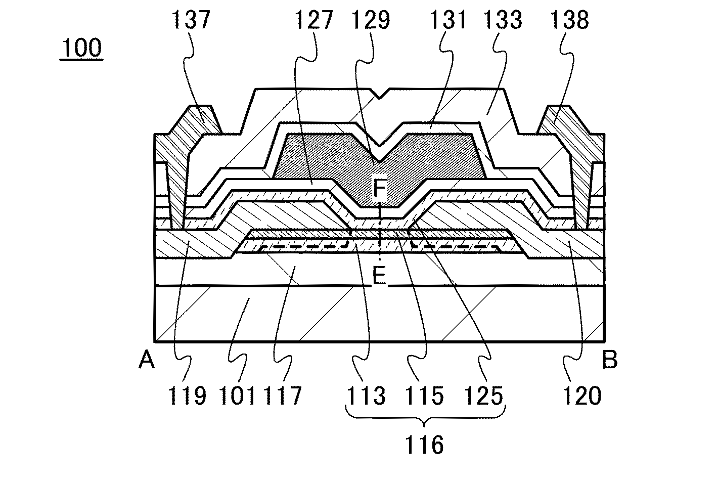
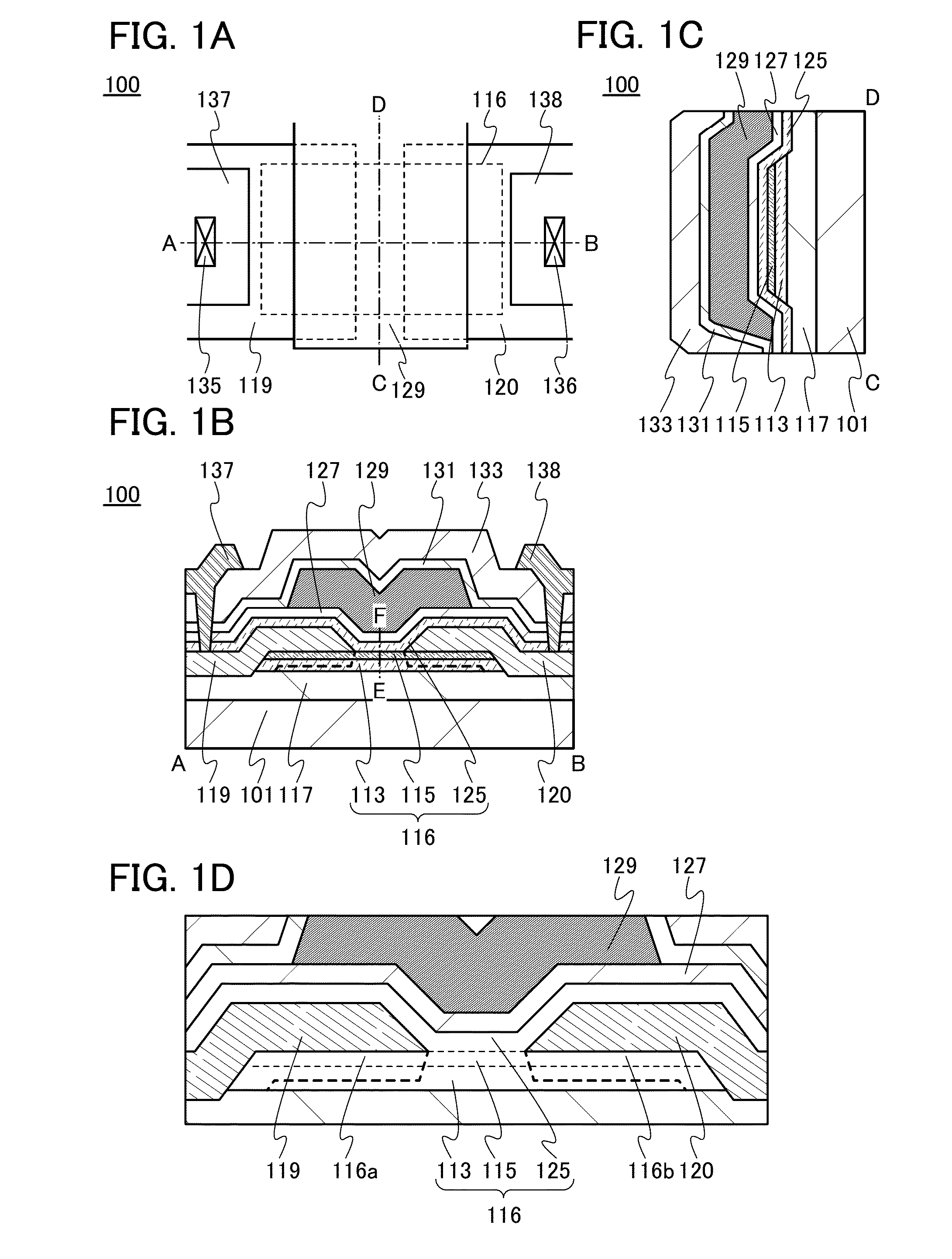
Semiconductor device and method for manufacturing the same
PatentPendingUS20240079502A1
Innovation
- A semiconductor device with a metal oxide layer containing indium and other metals, featuring a concentration gradient of oxygen and nitrogen, and a layered structure with varying crystallinity, is manufactured using a method that includes sequential deposition of the metal oxide layers in a vacuum environment to reduce oxygen vacancies and impurities, enhancing the electrical properties and reliability.


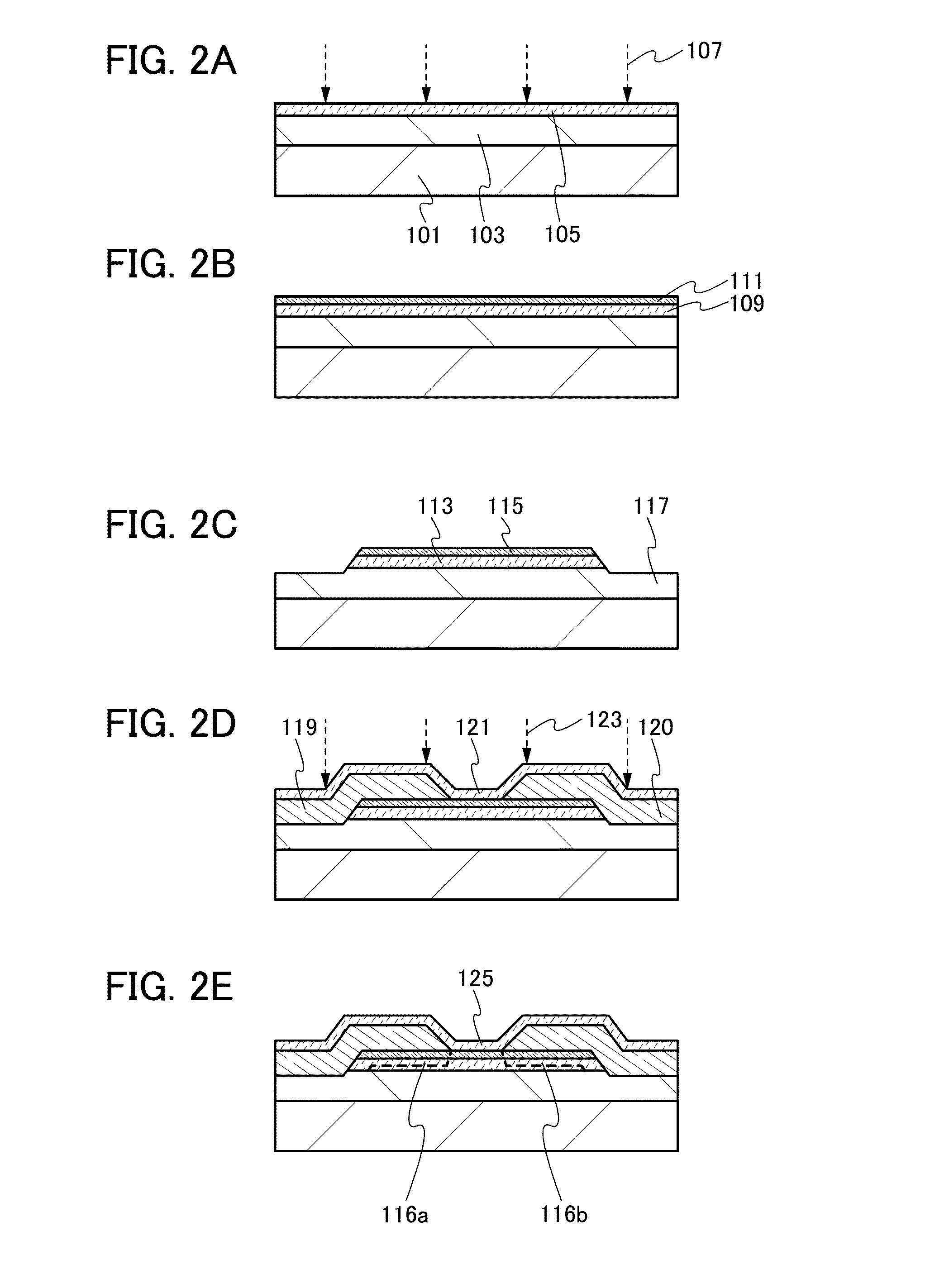
Method for manufacturing semiconductor device
PatentActiveUS20160254387A1
Innovation
- A transistor design that includes a first and second oxide film in contact with the oxide semiconductor film, where oxygen is added and diffused through heat treatment to reduce oxygen vacancies, using In-Ga-Zn oxide films with specific atomic ratios and compositions to improve electric characteristics and reliability.

Semiconductor Manufacturing Standards
Semiconductor manufacturing standards play a critical role in controlling iron oxide contamination and its effects on device performance. International organizations such as SEMI (Semiconductor Equipment and Materials International) and JEDEC (Joint Electron Device Engineering Council) have established comprehensive guidelines addressing metallic impurities in semiconductor fabrication. These standards define acceptable contamination levels, measurement methodologies, and quality control protocols specifically targeting transition metal contaminants including iron compounds.
The SEMI C1 standard specifies maximum allowable concentrations of metallic impurities on silicon wafer surfaces, with iron typically limited to 10^10 atoms/cm² for advanced technology nodes. For iron oxide particles, SEMI standards mandate rigorous monitoring through techniques such as Total Reflection X-Ray Fluorescence (TXRF) and Vapor Phase Decomposition Inductively Coupled Plasma Mass Spectrometry (VPD-ICP-MS). These measurement protocols ensure consistent detection sensitivity across different manufacturing facilities and equipment suppliers.
Cleanroom environmental standards, particularly ISO 14644 classifications, directly impact iron oxide contamination control. Class 1 and Class 10 cleanrooms required for advanced semiconductor manufacturing must maintain stringent airborne particle counts and implement specialized filtration systems to minimize iron-containing particulates. Material purity standards extend to process chemicals, with SEMI-grade specifications requiring iron content below parts-per-trillion levels in critical wet chemicals and gases.
Equipment qualification standards address iron contamination from manufacturing tools themselves. SEMI E10 guidelines for equipment assessment include protocols for evaluating metallic contamination contribution from process chambers, wafer handling systems, and chemical delivery infrastructure. Regular equipment baseline testing and preventive maintenance schedules are standardized to prevent iron oxide accumulation on contact surfaces.
Quality management systems compliant with ISO 9001 and automotive-specific IATF 16949 standards incorporate iron contamination monitoring as key process indicators. Statistical process control charts track contamination trends, triggering corrective actions when measurements approach specification limits. These standardized frameworks ensure consistent contamination management across global semiconductor supply chains, enabling reliable performance outcomes in iron-sensitive device applications.
Environmental Impact Assessment
The semiconductor manufacturing industry's environmental footprint has come under increasing scrutiny as global sustainability standards tighten. Iron oxide contamination in semiconductor fabrication facilities presents multifaceted environmental challenges that extend beyond production efficiency concerns. The primary environmental impact stems from wastewater treatment processes, where iron oxide particles require specialized filtration and chemical treatment protocols. These treatment procedures generate secondary waste streams containing concentrated metal compounds, necessitating careful disposal management to prevent soil and groundwater contamination.
Energy consumption represents another critical environmental dimension. When iron oxide contamination occurs, affected semiconductor wafers often require additional cleaning cycles and reprocessing steps, substantially increasing energy usage per functional unit produced. Studies indicate that contamination-related rework can elevate energy consumption by 15-30% for affected production batches. This energy penalty translates directly into increased carbon emissions, particularly in regions where semiconductor manufacturing relies heavily on fossil fuel-based electricity generation.
Chemical usage intensification poses significant environmental concerns. Removing iron oxide contamination demands aggressive cleaning agents, including acidic solutions and organic solvents, which increase the volume of hazardous chemical waste requiring treatment. The semiconductor industry already ranks among the most chemical-intensive manufacturing sectors, and contamination incidents exacerbate this environmental burden. Proper neutralization and disposal of these chemicals require sophisticated waste management infrastructure and ongoing monitoring to ensure regulatory compliance.
Material waste generation constitutes a substantial environmental impact. Semiconductor wafers contaminated beyond recovery thresholds must be scrapped, representing not only economic loss but also environmental waste of the rare earth elements, ultra-pure silicon, and other valuable materials embedded in these substrates. The cumulative effect of contamination-related scrap contributes to resource depletion concerns and increases the industry's overall material intensity ratio. Implementing robust contamination prevention strategies therefore serves dual purposes: enhancing production efficiency while simultaneously reducing environmental impact through decreased waste generation, lower energy consumption, and minimized chemical usage.
Unlock deeper insights with Patsnap Eureka Quick Research — get a full tech report to explore trends and direct your research. Try now!
Generate Your Research Report Instantly with AI Agent
Supercharge your innovation with Patsnap Eureka AI Agent Platform!