

Analyzing Metal Gate Work Function in Nanosheet Transistors
APR 23, 20269 MIN READ
Generate Your Research Report Instantly with AI Agent
PatSnap Eureka helps you evaluate technical feasibility & market potential.
Metal Gate Work Function in Nanosheet Transistor Background
The evolution of semiconductor technology has reached a critical juncture where traditional planar transistor architectures face fundamental physical limitations in scaling beyond the 7nm technology node. As Moore's Law approaches its theoretical boundaries, the semiconductor industry has pivoted toward three-dimensional transistor structures to maintain performance improvements while continuing dimensional scaling. Nanosheet transistors represent the latest advancement in this evolutionary path, emerging as the successor to FinFET technology for sub-3nm process nodes.
Nanosheet transistors, also known as Gate-All-Around (GAA) transistors, fundamentally differ from their predecessors by completely surrounding the channel material with gate electrodes. This architectural innovation provides superior electrostatic control over the channel, significantly reducing short-channel effects and leakage currents that plague scaled planar and FinFET devices. The technology enables continued scaling while maintaining or improving device performance metrics such as drive current, subthreshold swing, and DIBL (Drain-Induced Barrier Lowering).
The metal gate work function emerges as a critical parameter in nanosheet transistor design due to the unique geometric constraints and enhanced gate coupling inherent in the GAA structure. Unlike planar transistors where work function engineering primarily affects threshold voltage control, nanosheet devices require precise work function tuning to optimize multiple performance parameters simultaneously. The complete gate wrap-around geometry amplifies the impact of work function variations on device characteristics, making accurate analysis and control essential for reliable circuit operation.
Historical development of work function engineering began with the introduction of high-k/metal gate stacks in the 45nm technology generation, initially addressing gate leakage and polysilicon depletion issues. The transition from polysilicon gates to metal gates necessitated the development of materials with tunable work functions to achieve appropriate threshold voltages for both NMOS and PMOS devices. This dual work function approach became the foundation for modern CMOS technology, enabling continued scaling while maintaining device performance.
The primary objective of analyzing metal gate work function in nanosheet transistors encompasses several critical aspects: establishing accurate measurement methodologies for the unique GAA geometry, understanding work function uniformity across multiple nanosheets within a single device, and developing predictive models for work function impact on device performance. Additionally, the analysis aims to identify optimal work function values for different circuit applications and establish process control requirements for manufacturing consistency.
Current technological goals focus on achieving work function control within ±10mV across wafer-scale manufacturing, developing in-line measurement techniques for process monitoring, and establishing correlation between work function variations and final device performance metrics. These objectives directly support the broader industry goal of successful nanosheet transistor implementation in high-volume manufacturing for advanced logic and memory applications.
Market Demand for Advanced Nanosheet Transistor Technology
The semiconductor industry is experiencing unprecedented demand for advanced nanosheet transistor technology, driven by the relentless pursuit of Moore's Law continuation and the exponential growth in computational requirements across multiple sectors. This demand stems from the fundamental limitations of conventional FinFET technology, which is approaching its scaling limits at advanced nodes below 3nm.
Data centers and cloud computing infrastructure represent the largest market segment driving nanosheet transistor adoption. The explosive growth in artificial intelligence, machine learning, and high-performance computing applications requires processors with superior power efficiency and performance density. Nanosheet transistors, with their enhanced gate control and reduced short-channel effects, offer the necessary improvements in drive current and power consumption that these applications demand.
Mobile device manufacturers constitute another critical demand driver, as consumer expectations for battery life, processing speed, and device miniaturization continue to escalate. The superior electrostatic control achieved through nanosheet architecture enables better threshold voltage control and reduced leakage current, directly addressing the power efficiency requirements of mobile processors and system-on-chip designs.
The automotive sector's transition toward autonomous vehicles and electric mobility is creating substantial demand for advanced semiconductor solutions. Nanosheet transistors provide the reliability and performance characteristics essential for automotive-grade processors, particularly in applications requiring real-time processing capabilities and extended operational lifespans under harsh environmental conditions.
Emerging applications in Internet of Things devices, edge computing, and 5G infrastructure are expanding the addressable market for nanosheet technology. These applications require semiconductors that can deliver high performance while maintaining ultra-low power consumption, making the precise work function control in metal gate nanosheet transistors particularly valuable.
The market demand is further intensified by geopolitical factors and supply chain considerations, as nations and corporations seek to establish technological independence in critical semiconductor technologies. This has accelerated investment in advanced manufacturing capabilities and research initiatives focused on nanosheet transistor development.
Manufacturing cost considerations initially posed challenges to market adoption, but economies of scale and process maturation are gradually improving the cost-effectiveness proposition. The superior performance benefits and extended scaling roadmap offered by nanosheet technology justify the initial investment premiums for high-value applications.
Current Challenges in Metal Gate Work Function Control
Metal gate work function control in nanosheet transistors faces unprecedented challenges as device dimensions continue to shrink and architectural complexity increases. The transition from planar to three-dimensional nanosheet structures has introduced multiple technical barriers that significantly impact device performance and manufacturing yield. These challenges stem from the fundamental physics of ultra-thin materials, interface interactions, and the geometric constraints imposed by nanosheet architectures.
Interface stability represents one of the most critical challenges in nanosheet transistor metal gate systems. The high surface-to-volume ratio inherent in nanosheet structures amplifies interface effects, leading to increased sensitivity to contamination, oxidation, and interdiffusion between metal gate materials and the underlying gate dielectric. These interface phenomena can cause unpredictable work function shifts during processing and operation, compromising device reliability and performance consistency.
Thermal budget constraints during fabrication pose another significant obstacle. Traditional metal gate deposition and annealing processes often require elevated temperatures that can degrade the delicate nanosheet structures or cause unwanted material migration. The need to maintain structural integrity while achieving optimal work function values creates a narrow processing window that is difficult to control in high-volume manufacturing environments.
Uniformity control across multiple nanosheet layers presents unique engineering challenges. Each nanosheet within a stack may experience slightly different processing conditions due to shadowing effects, non-uniform precursor distribution, or varying stress states. This variability can result in work function variations between individual nanosheets within the same device, leading to threshold voltage dispersion and reduced device matching across arrays.
Material selection limitations further complicate work function engineering in nanosheet transistors. Many conventional metal gate materials that perform well in planar devices exhibit poor conformality or adhesion on nanosheet surfaces. The requirement for atomic-level thickness control and the need to maintain electrical continuity around sharp nanosheet edges restrict the available material palette and processing techniques.
Characterization and metrology challenges also impede progress in work function control. Traditional electrical measurement techniques may not provide sufficient spatial resolution to isolate individual nanosheet contributions to overall device behavior. Advanced analytical methods are required to correlate local work function variations with device performance, but these techniques often lack the throughput necessary for manufacturing process development and control.
Existing Metal Gate Work Function Tuning Solutions
01 Metal gate electrode materials with tunable work function
Various metal materials and metal alloys can be used as gate electrodes in semiconductor devices, where the work function can be tuned by adjusting the composition, thickness, or processing conditions. These materials include transition metals, metal nitrides, and metal carbides that provide different work function values suitable for NMOS or PMOS transistors. The selection and engineering of these materials enable optimization of threshold voltage and device performance.- Metal gate electrode materials with tunable work function: Various metal materials and metal alloys can be used as gate electrodes in semiconductor devices, where the work function can be tuned by adjusting the composition, thickness, or processing conditions. These materials include transition metals, metal nitrides, and metal carbides that provide different work function values suitable for NMOS or PMOS transistors. The selection and engineering of these materials enable optimization of threshold voltage and device performance.
- Work function adjustment through doping and alloying: The work function of metal gate electrodes can be modified by incorporating dopants or forming alloys with specific elements. This approach allows fine-tuning of the work function to achieve desired threshold voltages in transistor devices. Different doping concentrations and alloy compositions provide a range of work function values, enabling the fabrication of complementary devices with optimized electrical characteristics.
- Multi-layer metal gate structures for work function engineering: Stacked or multi-layer metal gate structures can be employed to achieve specific work function values and improve device performance. These structures may include combinations of different metal layers, barrier layers, and capping layers that collectively determine the effective work function. The multi-layer approach provides flexibility in work function tuning while addressing issues such as thermal stability and interface quality.
- Work function modulation through thermal treatment and annealing: Thermal processing techniques such as annealing can be used to modify the work function of metal gate electrodes. The temperature, duration, and ambient conditions of thermal treatment affect the crystalline structure, phase composition, and interfacial properties of the metal gate, thereby altering its work function. This method enables post-deposition adjustment of work function to meet specific device requirements.
- Integration of metal gates with high-k dielectrics for work function optimization: The combination of metal gate electrodes with high-k dielectric materials requires careful consideration of work function matching and interface engineering. The interaction between the metal gate and high-k dielectric can influence the effective work function through interface dipole formation and charge transfer effects. Proper selection of metal-dielectric combinations and processing methods ensures optimal work function alignment and device performance in advanced transistor technologies.
02 Work function adjustment through metal layer stacking
Multiple metal layers can be stacked in a gate structure to achieve desired work function values. By combining different metal materials in a layered configuration, the effective work function can be controlled and optimized. This approach allows for fine-tuning of electrical characteristics and enables the fabrication of devices with specific threshold voltage requirements. The thickness and sequence of the metal layers play crucial roles in determining the final work function.Expand Specific Solutions03 Work function modulation through doping and alloying
The work function of metal gate electrodes can be modified by introducing dopants or creating metal alloys. Incorporating specific elements into the metal gate material changes its electronic properties and shifts the work function to desired values. This technique enables precise control over device characteristics and allows for the creation of both high and low work function gates on the same substrate. Various doping concentrations and alloy compositions can be employed to achieve target work function values.Expand Specific Solutions04 Interface engineering for work function control
The interface between the metal gate and the dielectric layer significantly affects the effective work function. By engineering the interface through surface treatments, insertion of interfacial layers, or controlled oxidation, the work function can be adjusted. These interface modifications influence charge distribution and band alignment, thereby tuning the electrical properties of the gate stack. Proper interface engineering is essential for achieving stable and reliable work function values.Expand Specific Solutions05 Thermal treatment effects on metal gate work function
Thermal processing steps such as annealing can significantly impact the work function of metal gate electrodes. The temperature, duration, and ambient conditions of thermal treatments affect the crystalline structure, grain size, and phase composition of the metal, which in turn influence the work function. Controlled thermal processing enables stabilization of the work function and optimization of device performance. Understanding and managing these thermal effects is critical for manufacturing reliable semiconductor devices.Expand Specific Solutions
Key Players in Nanosheet Transistor Development
The metal gate work function analysis in nanosheet transistors represents a critical technology area within the advanced semiconductor manufacturing industry, currently in a mature development stage driven by the transition to sub-3nm process nodes. The market demonstrates substantial scale with major foundries like TSMC, Samsung Electronics, and SMIC leading manufacturing capabilities, while equipment suppliers including Tokyo Electron and ASM International provide essential fabrication tools. Technology maturity varies significantly across players, with TSMC and Samsung achieving production-ready implementations, Intel and IBM driving research innovations, and emerging companies like Rapidus pursuing catch-up strategies. Chinese entities including SMIC and various research institutes are rapidly advancing their capabilities, while established players like Infineon and GlobalFoundries focus on specialized applications, creating a highly competitive landscape with distinct technological and geographical clusters.
International Business Machines Corp.
Technical Solution: IBM has pioneered innovative metal gate work function engineering approaches for nanosheet transistors through their research collaborations and advanced technology development programs. Their methodology focuses on novel metal alloy compositions and interface engineering techniques to achieve precise work function tuning. IBM's research includes exploration of alternative metal systems beyond traditional TiN-based approaches, investigating materials like TaCN and other transition metal compounds. The company has developed comprehensive modeling frameworks for predicting work function behavior in nanosheet geometries and has contributed significantly to understanding the fundamental physics of metal-semiconductor interfaces in these advanced structures.
Strengths: Strong research capabilities and fundamental understanding of device physics with innovative material solutions. Weaknesses: Limited manufacturing scale compared to pure-play foundries and higher research-to-production transition costs.
Samsung Electronics Co., Ltd.
Technical Solution: Samsung has developed advanced metal gate work function engineering for nanosheet transistors using dual work function metal integration. Their approach employs TiN-based metal gates with precise thickness control and optimized annealing processes to achieve target threshold voltages for both NMOS and PMOS devices. The company utilizes atomic layer deposition (ALD) techniques for conformal metal gate deposition around nanosheet structures, ensuring uniform work function distribution. Samsung's process includes work function tuning through nitrogen incorporation and thermal budget optimization, achieving effective work function values ranging from 4.1-4.9 eV for different device types.
Strengths: Industry-leading manufacturing capabilities and extensive experience in advanced node production. Weaknesses: High manufacturing complexity and cost associated with dual metal gate processes.
Core Innovations in Work Function Analysis Methods
Method for tuning the work function of a metal gate of the PMOS device
PatentActiveUS8367558B2
Innovation
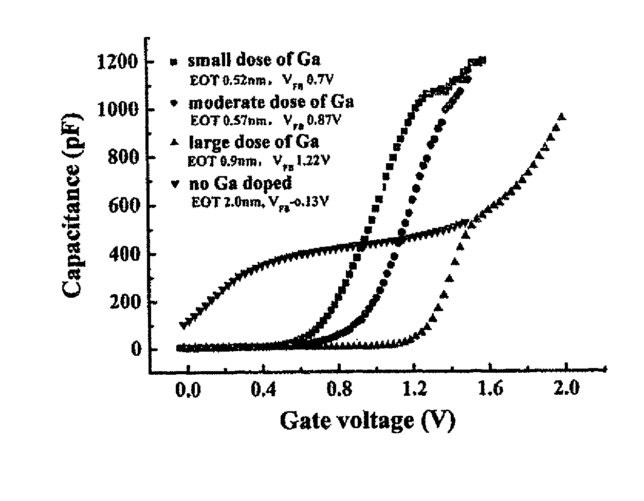
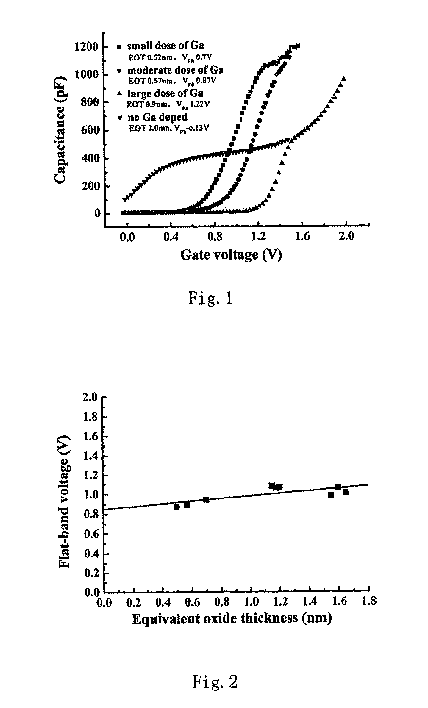
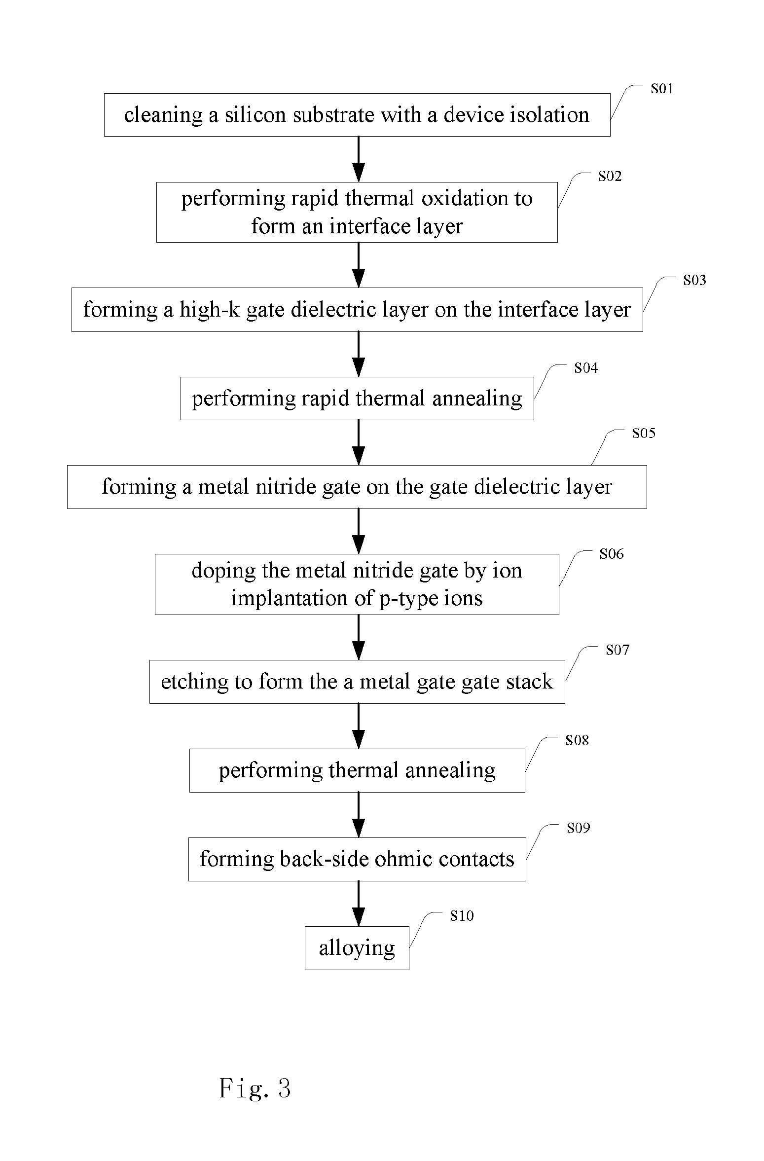
- The method involves depositing a metal nitride or metal layer on a high-k gate dielectric, doping with ions like Al, Pt, Ru, or Ga through ion implantation, and performing rapid high-temperature annealing to accumulate doped ions at the interface or generate dipoles, thereby tuning the work function of the metal gate.
Dual metal gates for mugfet device
PatentActiveUS7582521B2
Innovation
- A method involving the formation of metal gate electrodes by reacting a first-metal-containing material with a second-metal-containing material on a gate dielectric, using materials like Al2O3 and TaN, TiN, WN, or MoN to achieve a work function value ranging from 4.35 eV to 5.0 eV, applicable to both PMOS and NMOS transistors, including three-dimensional FinFET devices.


Semiconductor Manufacturing Process Considerations
The manufacturing of nanosheet transistors with precise metal gate work function control presents significant process challenges that require careful consideration of multiple fabrication parameters. The atomic-scale dimensions of these devices demand unprecedented precision in material deposition, etching, and thermal processing steps.
Gate stack formation represents the most critical manufacturing consideration, where atomic layer deposition (ALD) techniques must achieve uniform coverage across the complex three-dimensional nanosheet geometry. The conformal deposition of high-k dielectrics and metal gate materials requires optimized precursor chemistry and process conditions to ensure consistent thickness and composition throughout the channel region. Temperature control during ALD becomes particularly crucial as thermal budgets directly impact work function stability and interface quality.
The sequential release and gate formation process introduces unique challenges in maintaining structural integrity while achieving the desired electrical characteristics. Selective etching processes must precisely remove sacrificial layers without damaging the silicon nanosheets or compromising the gate dielectric integrity. Process-induced stress and thermal cycling during manufacturing can significantly alter the work function properties of metal gates, necessitating careful optimization of annealing conditions and ambient environments.
Contamination control emerges as a paramount concern due to the increased surface area and complexity of nanosheet structures. Even trace amounts of impurities can dramatically affect work function values and device performance variability. Clean room protocols must be enhanced to address the unique contamination pathways associated with high aspect ratio structures and multiple material interfaces.
Process monitoring and metrology present additional challenges, as traditional measurement techniques may not provide adequate sensitivity or spatial resolution for nanosheet geometries. Advanced characterization methods, including electron beam techniques and scanning probe microscopy, become essential for verifying work function uniformity and identifying process-related variations. The development of inline monitoring capabilities remains crucial for maintaining manufacturing yield and device performance consistency across wafer-scale production.
Reliability and Performance Impact Assessment
The reliability and performance impact of metal gate work function variations in nanosheet transistors represents a critical concern for advanced semiconductor manufacturing. Work function fluctuations directly influence threshold voltage stability, which subsequently affects device reliability over extended operational periods. Statistical variations in work function across different transistor instances can lead to significant performance degradation, particularly in high-density integrated circuits where uniformity is paramount.
Threshold voltage shifts caused by work function instability manifest as increased leakage currents and reduced switching speeds. These variations become more pronounced under stress conditions such as elevated temperatures, high electric fields, and prolonged operational cycles. The impact is particularly severe in nanosheet architectures due to their increased surface-to-volume ratio, which amplifies the sensitivity to interface states and charge trapping phenomena.
Performance metrics including drive current, subthreshold swing, and drain-induced barrier lowering exhibit strong correlations with work function consistency. Devices with optimized work function alignment demonstrate superior electrostatic control and reduced short-channel effects. However, process-induced variations can result in performance spreads that compromise circuit yield and operational margins.
Reliability assessment reveals that work function degradation mechanisms include metal interdiffusion, oxygen vacancy migration, and interface roughening. These phenomena contribute to time-dependent threshold voltage shifts and potential device failure modes. The reliability impact becomes more critical as device dimensions scale down, requiring enhanced process control and material engineering approaches.
Long-term stability analysis indicates that proper work function engineering can extend device lifetime by minimizing bias temperature instability and hot carrier effects. The performance-reliability trade-offs necessitate careful optimization of metal gate composition, interface engineering, and thermal budget management to achieve acceptable device specifications while maintaining manufacturing feasibility.
Unlock deeper insights with PatSnap Eureka Quick Research — get a full tech report to explore trends and direct your research. Try now!
Generate Your Research Report Instantly with AI Agent
Supercharge your innovation with PatSnap Eureka AI Agent Platform!