Breakthroughs in all-passive network components with silicon photonics.
JUL 17, 20259 MIN READ
Generate Your Research Report Instantly with AI Agent
PatSnap Eureka helps you evaluate technical feasibility & market potential.
Silicon Photonics Evolution and Objectives
Silicon photonics has emerged as a transformative technology in the field of integrated optics, revolutionizing the way we approach optical communication and data processing. The evolution of silicon photonics can be traced back to the early 2000s when researchers began exploring the potential of using silicon as a platform for photonic devices. This breakthrough was driven by the need for higher bandwidth, lower power consumption, and increased integration density in optical communication systems.
The primary objective of silicon photonics is to leverage the well-established semiconductor manufacturing infrastructure to produce photonic components and circuits on a silicon substrate. This approach aims to combine the benefits of optical communication with the scalability and cost-effectiveness of silicon-based electronics. By integrating optical and electronic components on a single chip, silicon photonics promises to overcome the limitations of traditional copper-based interconnects and enable faster, more efficient data transmission.
Over the past two decades, silicon photonics has made significant strides in addressing key challenges such as light generation, modulation, detection, and routing on a silicon platform. The development of passive components, including waveguides, couplers, and filters, has been crucial in enabling the creation of complex photonic circuits. These advancements have paved the way for the realization of all-passive network components, which offer advantages in terms of power efficiency and reliability.
The evolution of silicon photonics has been marked by several key milestones. These include the demonstration of high-speed silicon modulators, the integration of germanium photodetectors on silicon, and the development of efficient coupling techniques between optical fibers and silicon waveguides. More recently, researchers have focused on enhancing the performance of passive components, exploring novel designs and materials to minimize losses and improve functionality.
Looking ahead, the objectives of silicon photonics in the context of all-passive network components are multifaceted. One primary goal is to further reduce propagation losses in silicon waveguides, enabling longer-distance on-chip communication. Another objective is to develop more efficient and compact passive devices, such as wavelength-division multiplexers and optical switches, to support higher data rates and more complex network architectures.
Additionally, researchers are working towards improving the integration density of passive components, allowing for more functionality to be packed into smaller chip areas. This includes the development of 3D integration techniques and the exploration of new materials that can be seamlessly integrated with silicon. The ultimate aim is to create highly scalable, low-cost photonic integrated circuits that can meet the ever-increasing demands of data centers, telecommunications networks, and emerging applications in areas such as artificial intelligence and quantum computing.
Market Demand for Passive Optical Networks
The demand for passive optical networks (PONs) has been steadily increasing due to the growing need for high-speed, reliable, and cost-effective broadband connectivity. This market growth is primarily driven by the rising adoption of fiber-to-the-home (FTTH) and fiber-to-the-building (FTTB) technologies, which require extensive deployment of passive optical components.
The global PON market is experiencing significant expansion, with a compound annual growth rate (CAGR) projected to remain strong in the coming years. This growth is fueled by several factors, including the increasing demand for high-bandwidth applications, the proliferation of smart devices, and the ongoing digital transformation across various industries.
Telecommunications service providers are investing heavily in PON infrastructure to meet the escalating demand for faster internet speeds and improved network reliability. This trend is particularly evident in emerging economies, where rapid urbanization and growing middle-class populations are driving the need for advanced communication networks.
The enterprise sector is also contributing to the market demand for PONs, as businesses seek to enhance their network capabilities to support cloud computing, big data analytics, and Internet of Things (IoT) applications. PONs offer advantages such as reduced power consumption, lower maintenance costs, and improved scalability compared to traditional copper-based networks.
Government initiatives and regulations promoting broadband access in rural and underserved areas are further stimulating the demand for PON technologies. Many countries have set ambitious targets for nationwide broadband coverage, which is expected to drive substantial investments in passive optical network infrastructure.
The advent of 5G technology is creating new opportunities for PON market growth. As mobile network operators deploy dense small cell networks to support 5G services, there is an increasing need for fiber backhaul solutions, where PONs can play a crucial role in providing cost-effective and high-capacity connectivity.
The integration of silicon photonics in passive network components is poised to revolutionize the PON market. This technology offers the potential for miniaturization, improved performance, and reduced costs of optical components, which could lead to more widespread adoption of PON solutions across various sectors.
As the demand for bandwidth-intensive applications continues to grow, there is an increasing interest in next-generation PON technologies, such as XG-PON, XGS-PON, and NG-PON2. These advanced systems promise higher data rates and improved network efficiency, further driving the market demand for passive optical networks.
Current Challenges in All-Passive Components
Despite significant advancements in silicon photonics, all-passive network components still face several critical challenges that hinder their widespread adoption and optimal performance. One of the primary obstacles is the inherent propagation loss in silicon waveguides. While silicon offers excellent light confinement, it suffers from higher absorption and scattering losses compared to traditional optical fibers, especially at longer wavelengths. This limitation impacts the overall efficiency and scalability of passive photonic circuits.
Another major challenge lies in the precise control of light propagation and manipulation within passive components. Achieving accurate phase control, polarization management, and mode conversion in compact silicon structures remains difficult due to fabrication tolerances and environmental sensitivities. These factors can lead to performance variations and reduced reliability in complex photonic circuits.
The integration of multiple passive functions into a single compact device presents yet another hurdle. As photonic circuits become more sophisticated, there is a growing need for multifunctional components that can perform tasks such as splitting, filtering, and routing simultaneously. However, designing and fabricating such integrated devices while maintaining low loss and high performance across all functions is extremely challenging.
Temperature sensitivity is a persistent issue in silicon photonics, including passive components. The high thermo-optic coefficient of silicon causes significant wavelength shifts and performance fluctuations with temperature variations. This necessitates precise temperature control or the implementation of athermal designs, both of which add complexity and cost to the system.
Coupling efficiency between optical fibers and silicon waveguides remains a significant challenge. The mode size mismatch between standard optical fibers and silicon waveguides results in substantial coupling losses. While various coupling techniques have been developed, achieving high-efficiency, broadband, and polarization-insensitive coupling in a compact form factor is still an ongoing research area.
Lastly, the manufacturing challenges associated with producing high-quality, low-loss passive components at scale cannot be overlooked. Current fabrication processes often result in sidewall roughness, dimensional variations, and material impurities that contribute to increased losses and performance degradation. Overcoming these manufacturing limitations is crucial for the widespread adoption of silicon photonics in practical applications.
Existing All-Passive Network Solutions
01 Passive optical components in silicon photonics
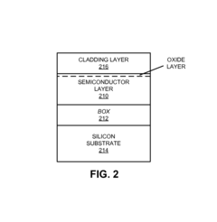
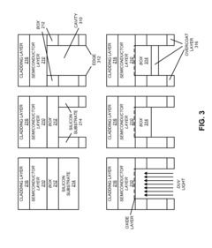
Silicon photonics technology enables the development of various passive optical components, such as waveguides, couplers, and splitters. These components are essential for routing and manipulating light signals within integrated photonic circuits, offering low-loss and compact solutions for optical networks.- Passive optical components in silicon photonics: Silicon photonics technology enables the creation of various passive optical components, such as waveguides, couplers, and splitters, on a single chip. These components are essential for routing and manipulating light signals in integrated photonic circuits, offering advantages like low loss, compact size, and compatibility with CMOS fabrication processes.
- All-passive optical network architectures: All-passive optical networks utilize only passive components for signal distribution, eliminating the need for active elements like amplifiers or switches. This approach reduces power consumption, improves reliability, and simplifies network maintenance. Silicon photonics enables the integration of multiple passive components on a single chip, making it ideal for implementing all-passive network architectures.
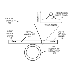
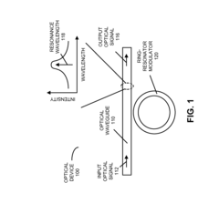
- Silicon photonic resonators and filters: Passive resonators and filters are crucial components in silicon photonic circuits. These structures, such as ring resonators and Bragg gratings, can be used for wavelength selection, filtering, and modulation in all-passive network designs. The high refractive index contrast in silicon allows for compact and efficient resonator designs with precise spectral characteristics.
- Passive optical interconnects: Silicon photonics enables the development of passive optical interconnects for high-speed data transmission within and between chips. These interconnects use waveguides, couplers, and other passive components to route optical signals, offering advantages such as high bandwidth, low latency, and reduced power consumption compared to traditional electrical interconnects.
- Integration of passive components with other materials: While silicon is the primary material for passive photonic components, integration with other materials can enhance functionality. For example, combining silicon with materials like germanium or III-V compounds allows for the creation of passive components with extended wavelength ranges or improved performance. This hybrid approach enables the development of more versatile all-passive network solutions.
02 All-passive optical network architectures
All-passive optical networks utilize only passive components for signal distribution and routing, eliminating the need for active elements like amplifiers or switches. This approach reduces power consumption, improves reliability, and simplifies network maintenance in silicon photonics-based systems.Expand Specific Solutions03 Integration of passive components on silicon substrates
Silicon photonics allows for the integration of multiple passive optical components on a single silicon substrate. This integration enables the creation of complex photonic circuits with reduced footprint and improved performance, suitable for various applications in optical communications and sensing.Expand Specific Solutions04 Passive wavelength division multiplexing (WDM) devices
Silicon photonics facilitates the development of passive WDM devices, such as arrayed waveguide gratings (AWGs) and echelle gratings. These components enable efficient multiplexing and demultiplexing of multiple wavelengths in all-passive optical networks, increasing data transmission capacity.Expand Specific Solutions05 Passive optical resonators and filters
Silicon photonics technology allows for the creation of passive optical resonators and filters, including ring resonators and Bragg gratings. These components play crucial roles in wavelength selection, filtering, and signal processing within all-passive optical networks, enhancing overall system performance.Expand Specific Solutions
Key Players in Silicon Photonics Industry
The silicon photonics market for all-passive network components is in a growth phase, with increasing demand driven by data center and telecommunications applications. The market size is expanding rapidly, expected to reach several billion dollars by 2025. Technologically, while still evolving, silicon photonics is maturing, with companies like Huawei, IBM, and Nokia leading innovation. Academic institutions such as MIT and Nanyang Technological University are also contributing significantly to research advancements. The competitive landscape is diverse, featuring established telecom giants, semiconductor manufacturers, and specialized photonics firms, all vying for market share in this promising field.
Huawei Technologies Co., Ltd.
Technical Solution: Huawei has made significant strides in silicon photonics for all-passive network components. Their approach involves integrating multiple passive optical functions onto a single chip, including waveguides, splitters, and filters. They have developed a silicon photonic integrated circuit (PIC) that can handle wavelength division multiplexing (WDM) with up to 96 channels[1]. This technology enables high-bandwidth data transmission with reduced power consumption and improved signal integrity. Huawei's all-passive components are designed to operate without the need for external power sources, relying on the inherent properties of silicon to manipulate light signals. Their latest breakthrough includes the development of ultra-low-loss silicon nitride waveguides, achieving losses as low as 0.1 dB/cm[2], which significantly enhances the performance of long-haul optical communications.
Strengths: High integration density, scalability for mass production, and compatibility with existing CMOS fabrication processes. Weaknesses: Challenges in coupling efficiency between optical fibers and on-chip waveguides, and potential thermal management issues in high-density designs.
Massachusetts Institute of Technology
Technical Solution: MIT's research in all-passive network components with silicon photonics focuses on developing novel structures and materials to enhance performance. They have pioneered the use of subwavelength grating structures in silicon waveguides to achieve ultra-low loss and precise control over light propagation[3]. MIT researchers have also developed all-passive optical routers using cascaded Mach-Zehnder interferometers, capable of routing multiple wavelengths simultaneously without active power consumption[4]. Their recent breakthrough involves the creation of photonic crystals with complete bandgaps in silicon, allowing for lossless light manipulation and the potential for all-optical computing[5]. Additionally, MIT has demonstrated all-passive wavelength conversion using four-wave mixing in silicon nanowires, achieving conversion efficiencies up to -1 dB across the C-band[6].
Strengths: Cutting-edge research in novel photonic structures, potential for revolutionary all-optical processing. Weaknesses: Some technologies may be far from commercial readiness, requiring further development for practical implementation.
Core Innovations in Silicon Photonics
Silicon photonics multi-channel parallel optical component and coupling method thereof
PatentActiveUS11740417B2
Innovation
- A silicon photonics integrated chip design that includes a laser group, FA assembly, and a coupling method with a PCBA board, thermal sink, and optical interface, utilizing a two-way DC laser and integrated receiving chip, along with a mature FA-MPO interface, to reduce costs and enhance integration, thereby lowering the material cost of parallel optical components.


Single-shot correction of resonant optical components
PatentActiveUS20160238791A1
Innovation
- A photonic chip with a substrate and semiconductor layer, where optical components are trimmed using localized low-temperature oxidation to achieve resonance wavelengths matching target values with high accuracy and stability without thermal or electronic tuning, utilizing deep-ultraviolet radiation and oxygen to modify the effective index of refraction.
Integration with Existing Fiber Networks
The integration of silicon photonics-based all-passive network components with existing fiber networks represents a critical challenge and opportunity in the evolution of telecommunications infrastructure. This integration process requires careful consideration of compatibility, performance, and cost-effectiveness to ensure seamless operation between legacy systems and cutting-edge silicon photonic technologies.
One of the primary advantages of silicon photonics is its potential for high-density integration and miniaturization. However, this also presents challenges when interfacing with traditional fiber optic networks, which operate at different scales and with different transmission characteristics. To bridge this gap, researchers and engineers have developed various transition technologies, such as spot-size converters and grating couplers, which enable efficient coupling between silicon waveguides and optical fibers.
The development of hybrid integration platforms has emerged as a promising approach to combining silicon photonics with existing fiber networks. These platforms allow for the co-packaging of silicon photonic chips with conventional optical components, creating a seamless interface between the two technologies. This approach not only facilitates integration but also enables the gradual adoption of silicon photonic technologies without requiring a complete overhaul of existing infrastructure.
Another key aspect of integration is the development of standardized interfaces and protocols that ensure interoperability between silicon photonic components and traditional fiber optic systems. Industry consortia and standards bodies are working to establish guidelines for interconnects, signal formats, and performance metrics that will enable smooth integration across different network architectures.
The integration process also involves addressing the differences in wavelength ranges and transmission formats between silicon photonics and traditional fiber networks. While many fiber networks operate in the C-band (1530-1565 nm), silicon photonics components often work best at slightly different wavelengths. Researchers are exploring ways to expand the operational range of silicon photonic devices to better align with existing fiber network specifications.
As integration efforts progress, there is a growing focus on developing hybrid systems that leverage the strengths of both silicon photonics and traditional fiber optics. For example, long-haul transmission may continue to rely on conventional fiber technology, while data centers and metro networks could increasingly adopt silicon photonic components for their superior integration density and energy efficiency.
The successful integration of silicon photonics with existing fiber networks holds the promise of significantly enhancing network capacity, reducing power consumption, and enabling new functionalities. However, it requires a carefully orchestrated approach that balances innovation with backward compatibility to ensure a smooth transition and widespread adoption across the telecommunications industry.
Energy Efficiency and Sustainability
Silicon photonics has emerged as a promising technology for addressing energy efficiency and sustainability challenges in optical networks. The integration of photonic components on silicon chips offers significant advantages in terms of power consumption, size reduction, and scalability. By leveraging the mature silicon manufacturing processes, all-passive network components can be produced with high yield and low cost, contributing to the overall sustainability of optical communication systems.
One of the key breakthroughs in all-passive network components with silicon photonics is the development of low-loss waveguides. These waveguides enable efficient light transmission within the chip, reducing power losses and improving overall energy efficiency. Advanced fabrication techniques, such as deep etching and sidewall smoothing, have led to waveguides with propagation losses as low as 0.1 dB/cm, significantly enhancing the performance of passive optical devices.
Another important advancement is the realization of high-performance passive optical filters using silicon photonics. These filters, including ring resonators and Bragg gratings, can be precisely engineered to achieve narrow bandwidth and low insertion loss. By eliminating the need for active components in filtering applications, power consumption is greatly reduced, contributing to the overall energy efficiency of optical networks.
The development of efficient fiber-to-chip couplers has also played a crucial role in improving the sustainability of silicon photonic devices. Grating couplers and edge couplers with coupling efficiencies exceeding 90% have been demonstrated, minimizing insertion losses at the interface between optical fibers and silicon chips. This breakthrough enables seamless integration of silicon photonic components into existing optical network infrastructures, reducing the need for additional amplification and power-hungry components.
Furthermore, the compact footprint of silicon photonic devices allows for higher integration density and reduced material usage. This not only leads to smaller and more energy-efficient network components but also contributes to the overall sustainability of the manufacturing process. The ability to integrate multiple functions on a single chip reduces the need for separate discrete components, simplifying system design and lowering power consumption.
In terms of thermal management, all-passive silicon photonic components offer inherent advantages. The absence of active elements eliminates the need for power-hungry cooling systems, further enhancing energy efficiency. Additionally, the high thermal conductivity of silicon allows for efficient heat dissipation, ensuring stable operation of passive devices without the need for external temperature control mechanisms.
Unlock deeper insights with PatSnap Eureka Quick Research — get a full tech report to explore trends and direct your research. Try now!
Generate Your Research Report Instantly with AI Agent
Supercharge your innovation with PatSnap Eureka AI Agent Platform!