

Chip Embedding in Flexible Electronics: How to Mitigate Delamination Risks
MAY 29, 20269 MIN READ
Generate Your Research Report Instantly with AI Agent
PatSnap Eureka helps you evaluate technical feasibility & market potential.
Flexible Electronics Chip Embedding Background and Objectives
Flexible electronics represents a paradigm shift in electronic device design, enabling the creation of bendable, stretchable, and conformable electronic systems that can adapt to curved surfaces and dynamic mechanical conditions. This revolutionary technology has emerged from decades of materials science advancement and manufacturing innovation, fundamentally challenging traditional rigid circuit board approaches. The evolution began with early polymer substrate research in the 1960s and has accelerated dramatically with recent breakthroughs in organic semiconductors, flexible displays, and wearable computing applications.
The integration of semiconductor chips into flexible substrates presents unique engineering challenges that differ significantly from conventional rigid electronics assembly. Traditional chip mounting techniques, designed for stable planar surfaces, become inadequate when substrates undergo repeated flexing, stretching, or twisting motions. The mechanical stress distribution, thermal expansion coefficients, and adhesion mechanisms all require fundamental reconsideration to ensure reliable long-term performance.
Delamination represents the most critical failure mode in flexible chip embedding applications, occurring when adhesive bonds between chips and flexible substrates deteriorate under mechanical stress. This phenomenon manifests through various mechanisms including interfacial crack propagation, adhesive fatigue, thermal cycling effects, and moisture-induced degradation. The consequences extend beyond simple mechanical failure to include electrical discontinuity, signal integrity degradation, and complete device malfunction.
Current market demands for flexible electronics span diverse applications including foldable smartphones, medical monitoring patches, automotive dashboard displays, and aerospace conformal antennas. Each application presents distinct mechanical requirements, environmental conditions, and reliability expectations that influence chip embedding strategies. The global flexible electronics market continues expanding rapidly, driven by consumer electronics innovation and emerging Internet of Things applications.
The primary technical objective focuses on developing robust chip embedding methodologies that maintain electrical and mechanical integrity throughout the operational lifetime of flexible electronic devices. This encompasses optimizing adhesive material selection, refining bonding process parameters, implementing stress-relief design features, and establishing predictive reliability assessment protocols. Success requires balancing competing requirements of flexibility, durability, electrical performance, and manufacturing scalability.
Secondary objectives include establishing standardized testing methodologies for delamination resistance evaluation, developing design guidelines for chip placement and interconnection strategies, and creating predictive models for failure mode analysis. These efforts aim to accelerate technology maturation and enable widespread commercial adoption across multiple industry sectors.
Market Demand for Reliable Flexible Electronic Devices
The global flexible electronics market is experiencing unprecedented growth driven by consumer demand for lightweight, bendable, and conformable electronic devices. Wearable technology represents the largest segment, with smartwatches, fitness trackers, and health monitoring patches requiring robust chip integration that can withstand repeated flexing without performance degradation. The healthcare sector particularly demands high reliability standards, as device failures in medical applications can have serious consequences for patient safety and treatment efficacy.
Consumer electronics manufacturers are increasingly incorporating flexible displays and sensors into smartphones, tablets, and emerging foldable devices. These applications require embedded chips that maintain electrical connectivity and mechanical integrity through thousands of bend cycles. The automotive industry presents another significant market opportunity, with flexible electronics enabling curved dashboard displays, seat-integrated sensors, and conformable lighting systems that must operate reliably in harsh environmental conditions.
Industrial Internet of Things applications are driving demand for flexible sensor networks that can be integrated into curved surfaces, pipelines, and machinery. These deployments require long-term reliability with minimal maintenance, making delamination prevention critical for operational continuity. The aerospace and defense sectors also require flexible electronics with exceptional reliability standards, where component failures can result in mission-critical system malfunctions.
Market research indicates that reliability concerns, particularly related to mechanical failures such as delamination, represent the primary barrier to broader flexible electronics adoption. End-users consistently prioritize device longevity and consistent performance over advanced features when mechanical reliability is compromised. This reliability imperative is creating substantial market pressure for improved chip embedding technologies that can eliminate delamination risks.
The convergence of 5G connectivity, edge computing, and miniaturization trends is further intensifying demand for reliable flexible electronics. These applications require embedded processors and communication chips that maintain signal integrity and thermal management while conforming to non-planar surfaces. Supply chain disruptions have also highlighted the importance of reliable manufacturing processes that minimize yield losses due to delamination-related defects.
Current Delamination Challenges in Flexible Chip Integration
Delamination represents one of the most critical failure modes in flexible chip integration, fundamentally challenging the reliability and longevity of flexible electronic systems. This phenomenon occurs when adhesive bonds between different material layers weaken or fail completely, leading to separation at critical interfaces. The primary concern lies in the interface between rigid silicon chips and flexible substrates, where significant material property mismatches create inherent stress concentrations.
Thermal cycling poses a substantial challenge due to the dramatic differences in coefficient of thermal expansion between silicon chips and flexible polymer substrates. Silicon typically exhibits a CTE of approximately 2.6 ppm/°C, while flexible substrates like polyimide can reach 20-40 ppm/°C. During temperature fluctuations, these mismatched expansion rates generate substantial interfacial stresses that progressively weaken adhesive bonds and promote crack initiation at chip edges.
Mechanical stress-induced delamination emerges as another critical challenge, particularly during bending operations that are fundamental to flexible electronics functionality. When flexible devices undergo bending, the embedded chips experience complex stress states including tension, compression, and shear forces. The rigid chip creates stress concentration points that exceed the adhesive strength limits, initiating delamination at chip corners and propagating along the chip perimeter.
Moisture ingress significantly exacerbates delamination risks by compromising adhesive integrity and creating additional expansion stresses. Flexible substrates are inherently more permeable to moisture compared to rigid PCBs, allowing water vapor to reach chip interfaces. This moisture absorption causes polymer swelling, reduces adhesive bond strength, and can lead to corrosion of metallization layers, further accelerating delamination processes.
Manufacturing process-induced challenges contribute substantially to delamination susceptibility. Inadequate surface preparation, contamination during assembly, and suboptimal curing conditions create weak interfacial bonds from the initial integration stage. The limited processing temperature windows for flexible substrates often prevent optimal adhesive curing, resulting in incomplete cross-linking and reduced bond strength.
Current detection and monitoring of delamination remain challenging due to the enclosed nature of embedded chips. Traditional inspection methods like visual examination or acoustic microscopy have limited effectiveness in identifying early-stage delamination in flexible assemblies. This detection difficulty often results in unnoticed progressive failure until complete functional breakdown occurs, highlighting the critical need for improved monitoring techniques and preventive design strategies.
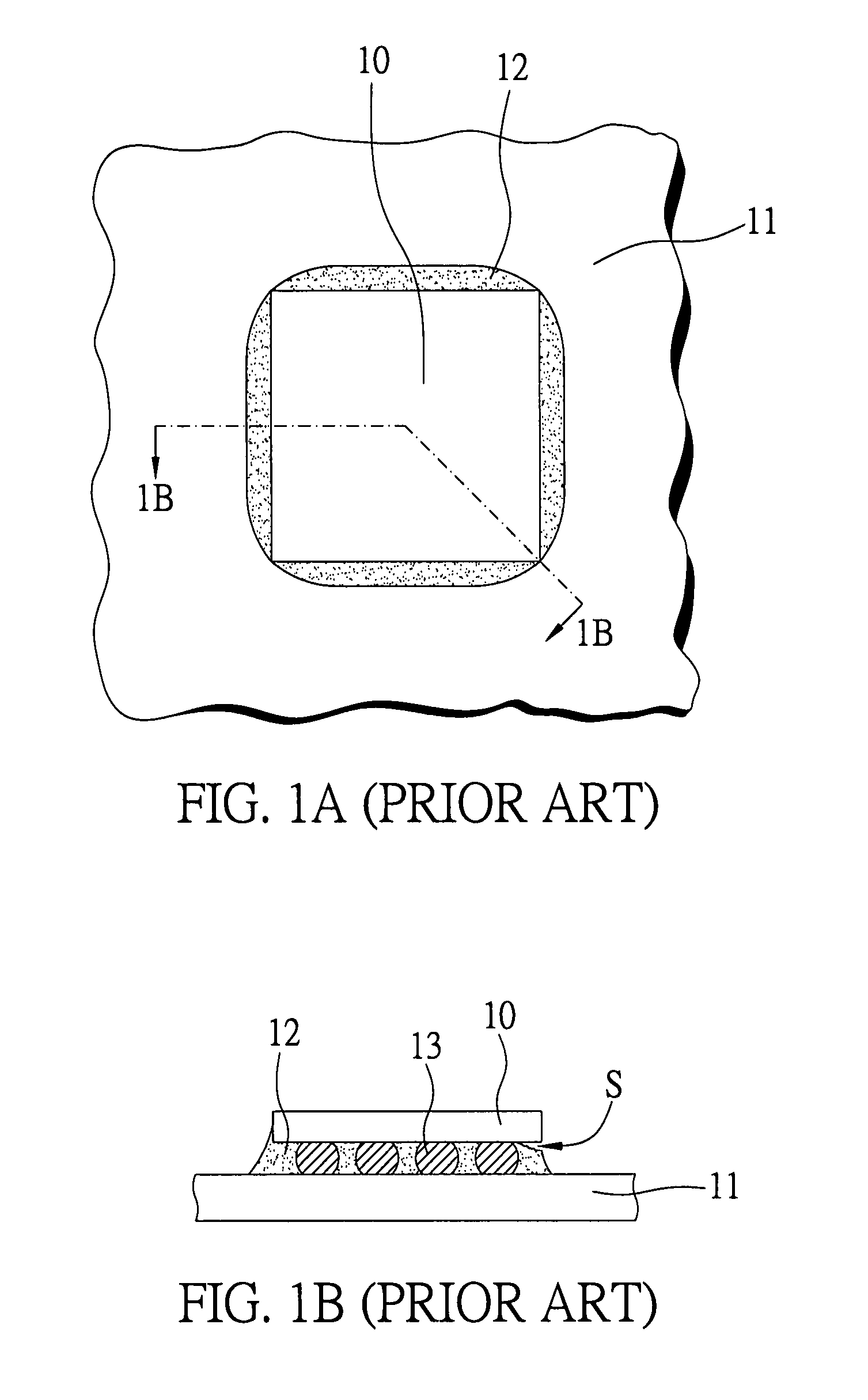
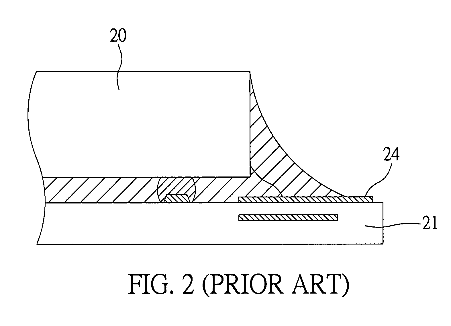
Existing Delamination Mitigation Solutions and Techniques
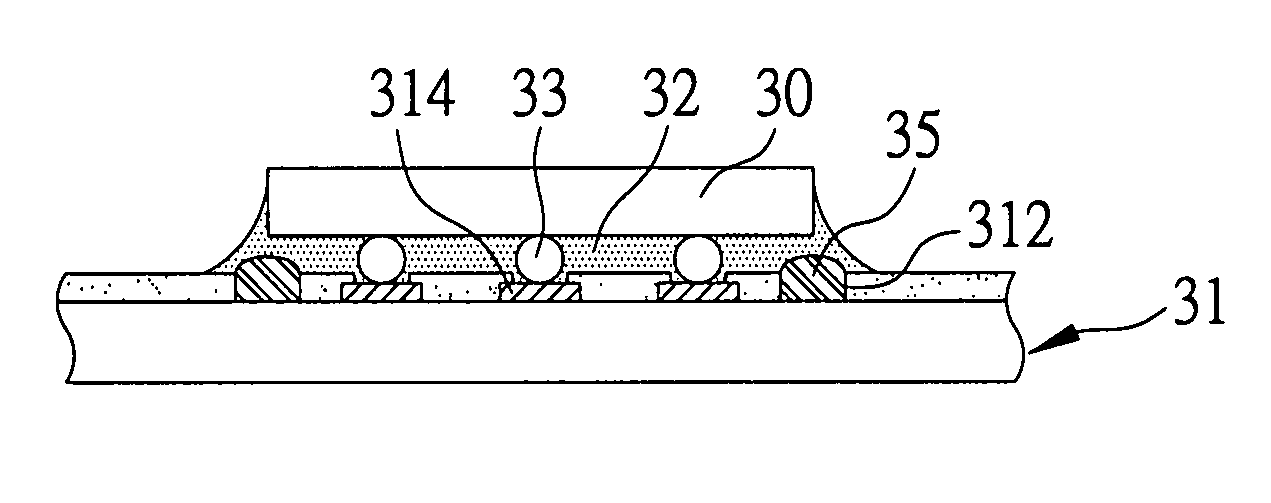
01 Adhesive layer improvement and bonding enhancement
Methods to improve the adhesive properties between chip and substrate through enhanced bonding materials, surface treatments, and adhesive layer modifications. These approaches focus on strengthening the interface connection to prevent delamination by optimizing adhesive composition and application techniques.- Adhesive layer optimization and bonding enhancement: Methods for improving the adhesive properties between chip and substrate through specialized bonding materials, surface treatments, and adhesive layer compositions. These techniques focus on enhancing the interfacial bonding strength to prevent delamination by optimizing the chemical and physical properties of the adhesive interface.
- Thermal stress management and coefficient matching: Approaches to reduce thermal-induced delamination by managing thermal expansion mismatches between different materials in the chip assembly. These solutions involve material selection, structural design modifications, and thermal management techniques to minimize stress concentrations that lead to delamination failures.
- Encapsulation material and molding compound improvements: Development of advanced encapsulation materials and molding compounds with enhanced adhesion properties and reduced shrinkage characteristics. These materials are designed to maintain strong bonds with chip surfaces while withstanding environmental stresses and manufacturing processes.
- Surface preparation and interface treatment methods: Techniques for preparing chip and substrate surfaces to improve adhesion and prevent delamination. These methods include surface roughening, chemical treatments, plasma processing, and application of coupling agents to create stronger interfacial bonds between materials.
- Structural design and mechanical reinforcement solutions: Design modifications and mechanical reinforcement strategies to prevent chip embedding delamination through improved structural integrity. These approaches include optimized package geometries, stress-relief features, and mechanical anchoring methods to distribute forces and prevent failure initiation.
02 Thermal stress management and heat dissipation
Techniques for managing thermal expansion mismatch and heat-induced stress that can cause delamination. Solutions include thermal interface materials, heat spreaders, and structural designs that accommodate thermal cycling while maintaining chip-substrate integrity.Expand Specific Solutions03 Mechanical reinforcement and structural support
Physical reinforcement methods including underfill materials, support structures, and mechanical anchoring systems to provide additional structural integrity. These solutions focus on distributing mechanical stress and preventing physical separation of embedded components.Expand Specific Solutions04 Surface preparation and interface optimization
Surface treatment methods and interface engineering techniques to improve adhesion between chip and embedding materials. These approaches include surface roughening, chemical treatments, and primer applications to create stronger interfacial bonds.Expand Specific Solutions05 Process control and manufacturing optimization
Manufacturing process improvements including curing conditions, pressure application, and quality control measures during chip embedding. These methods focus on optimizing processing parameters to minimize defects and ensure reliable chip-substrate bonding.Expand Specific Solutions
Key Players in Flexible Electronics and Chip Embedding Industry
The chip embedding in flexible electronics market is experiencing rapid growth driven by increasing demand for wearable devices, IoT applications, and bendable displays. The industry is transitioning from early development to commercial deployment phase, with market size projected to reach billions as consumer electronics embrace flexible form factors. Technology maturity varies significantly across players: established semiconductor giants like Samsung Electronics, Intel, and Taiwan Semiconductor Manufacturing demonstrate advanced packaging capabilities, while companies like Infineon Technologies and Texas Instruments contribute specialized power management solutions. Asian manufacturers including LG Display, Sharp, and Yangtze Memory Technologies are pioneering flexible substrate technologies. Research institutions like Tsinghua University and Carnegie Mellon University are advancing fundamental delamination mitigation techniques through novel adhesion materials and stress-relief designs, indicating strong academic-industry collaboration driving innovation forward.
Samsung Electronics Co., Ltd.
Technical Solution: Samsung has developed advanced chip embedding technologies for flexible electronics using ultra-thin chip packaging and specialized adhesive materials. Their approach involves reducing chip thickness to less than 50 micrometers and implementing multi-layer adhesion systems with thermoplastic polyurethane (TPU) and silicone-based encapsulants. The company utilizes laser-assisted bonding techniques and stress-relief structures around embedded chips to minimize mechanical stress during bending. Samsung's flexible OLED display technology incorporates embedded driver ICs using low-temperature polysilicon (LTPS) backplanes with optimized via structures and copper interconnects designed to withstand repeated flexing cycles.
Strengths: Industry-leading flexible display technology, extensive R&D resources, proven manufacturing capabilities. Weaknesses: High production costs, complex manufacturing processes requiring specialized equipment.
Intel Corp.
Technical Solution: Intel's approach to chip embedding in flexible electronics focuses on advanced packaging solutions including embedded wafer-level ball grid array (eWLB) technology and fan-out wafer-level packaging (FOWLP). Their methodology incorporates redistribution layers (RDL) with optimized copper trace designs and low-stress dielectric materials such as polyimide and benzocyclobutene (BCB). Intel has developed proprietary underfill materials with controlled coefficient of thermal expansion (CTE) matching and implements design rules for minimum bend radius specifications. The company's Foveros 3D packaging technology has been adapted for flexible substrates using through-silicon vias (TSVs) and micro-bump interconnections with enhanced reliability under mechanical stress.
Strengths: Advanced packaging expertise, strong materials science capabilities, robust testing methodologies. Weaknesses: Limited focus on consumer flexible electronics, primarily targets high-performance computing applications.
Core Innovations in Adhesion Enhancement for Chip Embedding
Electronic component with mechanically decoupled ball connections
PatentInactiveUS8324695B2
Innovation
- Incorporating mechanical decoupling means such as cavities and trenches in the chip and support layers, made from non-metallic materials, to absorb stresses and prevent delamination, along with the option of using viscous or plastic materials for additional damping and protection.


Flip-chip semiconductor package and chip carrier for preventing corner delamination
PatentActiveUS8207620B2
Innovation
- A chip carrier with a groove around the chip-mounting area filled with a low Young's modulus filler, combined with an underfill between the flip-chip and the carrier, to absorb and eliminate thermal stress, preventing delamination and providing support for the solder bumps.

Material Compatibility Standards for Flexible Electronics
Material compatibility standards for flexible electronics represent a critical framework for ensuring reliable chip embedding while minimizing delamination risks. These standards establish comprehensive guidelines for material selection, interface design, and performance validation across the entire flexible electronic system. The primary focus centers on thermal expansion coefficient matching, adhesion strength requirements, and chemical compatibility between different material layers.
The foundation of material compatibility lies in understanding the mechanical properties of substrate materials, adhesives, and encapsulants used in flexible electronics. Polyimide substrates, commonly used for their excellent thermal stability, require specific adhesion promoters to achieve optimal bonding with silicon chips. The coefficient of thermal expansion mismatch between rigid silicon and flexible substrates creates significant stress concentrations during temperature cycling, necessitating buffer layers or compliant interconnects.
Adhesive selection criteria encompass multiple performance parameters including peel strength, shear modulus, glass transition temperature, and moisture absorption characteristics. Epoxy-based adhesives typically provide superior mechanical strength but may exhibit brittleness under repeated flexing. Silicone-based alternatives offer enhanced flexibility but potentially lower adhesion strength, requiring careful optimization based on specific application requirements.
Interface engineering standards define surface preparation protocols, including plasma treatment, chemical etching, and primer application procedures. These processes ensure consistent surface energy and promote molecular-level bonding between dissimilar materials. Standardized test methods evaluate interfacial adhesion through pull tests, lap shear measurements, and environmental stress screening protocols.
Environmental compatibility requirements address moisture sensitivity, chemical resistance, and UV stability of material combinations. Flexible electronics often operate in harsh conditions where temperature fluctuations, humidity exposure, and mechanical stress occur simultaneously. Material standards specify accelerated aging tests that simulate real-world operating conditions to validate long-term reliability.
Quality assurance protocols incorporate statistical process control methods for material characterization and batch-to-batch consistency verification. These standards ensure reproducible manufacturing outcomes and enable predictive modeling of delamination failure modes across different material combinations and processing conditions.
Reliability Testing Protocols for Embedded Chip Systems
Establishing comprehensive reliability testing protocols for embedded chip systems in flexible electronics requires a multi-faceted approach that addresses the unique challenges posed by mechanical flexibility and thermal cycling. The primary focus centers on developing standardized test methodologies that can accurately predict long-term performance under real-world operating conditions while specifically targeting delamination failure modes.
Mechanical stress testing protocols form the cornerstone of reliability assessment for flexible embedded systems. These protocols must incorporate cyclic bending tests with varying radii of curvature, ranging from 10mm to 50mm, to simulate different application scenarios. The testing should include both static bending holds and dynamic flexing cycles, with frequencies typically ranging from 0.1Hz to 10Hz depending on the intended application. Critical parameters to monitor include interfacial resistance changes, optical inspection for crack initiation, and acoustic emission detection for early delamination warning signs.
Thermal cycling protocols require careful consideration of the coefficient of thermal expansion mismatches between chip materials and flexible substrates. Standard temperature ranges should span from -40°C to +85°C for consumer applications, with extended ranges up to 125°C for automotive applications. The protocols must include rapid temperature transitions to induce maximum thermal stress, combined with extended dwell times to assess creep behavior. Simultaneous mechanical flexing during thermal cycling provides crucial insights into combined stress effects that often trigger delamination failures.
Environmental stress screening protocols encompass humidity testing, chemical exposure assessment, and UV degradation evaluation. Humidity testing should follow modified versions of JEDEC standards, adapted for flexible substrates with 85°C/85% relative humidity conditions extended to account for the increased permeability of flexible materials. Chemical resistance testing must evaluate exposure to common solvents, cleaning agents, and bodily fluids for wearable applications.
Accelerated life testing methodologies require careful calibration to ensure correlation with actual field performance. The Arrhenius model provides a foundation for temperature acceleration, while mechanical acceleration factors must be established through extensive correlation studies. Weibull analysis becomes essential for characterizing failure distributions and establishing confidence intervals for reliability predictions.
Real-time monitoring capabilities during testing enable early detection of degradation mechanisms before catastrophic failure occurs. In-situ resistance monitoring, impedance spectroscopy, and high-resolution imaging techniques provide continuous assessment of interface integrity. These monitoring systems must be integrated into automated test platforms capable of handling large sample sizes while maintaining precise control over environmental and mechanical stress conditions.
Unlock deeper insights with PatSnap Eureka Quick Research — get a full tech report to explore trends and direct your research. Try now!
Generate Your Research Report Instantly with AI Agent
Supercharge your innovation with PatSnap Eureka AI Agent Platform!