

Comparing Plasma Vs Ion Beam Methods For Cleaning Electrostatic Chucks
MAY 14, 20269 MIN READ
Generate Your Research Report Instantly with AI Agent
PatSnap Eureka helps you evaluate technical feasibility & market potential.
Plasma and Ion Beam Cleaning Technology Background and Objectives
Electrostatic chucks (ESCs) have become indispensable components in semiconductor manufacturing processes, serving as critical wafer holding mechanisms in plasma etching, ion implantation, and chemical vapor deposition systems. These devices utilize electrostatic forces to secure wafers during processing, eliminating the need for mechanical clamping that could cause wafer damage or contamination. However, the operational environment of ESCs presents significant challenges, as they are continuously exposed to reactive plasma species, process gases, and byproduct deposition that gradually accumulate on their surfaces.
The contamination of ESC surfaces represents a fundamental challenge in semiconductor fabrication, directly impacting process yield, wafer quality, and equipment uptime. Organic residues, metal particles, and polymer deposits can alter the electrostatic field distribution, leading to non-uniform wafer clamping forces and potential wafer breakage. Additionally, contaminated surfaces can introduce unwanted chemical reactions during subsequent processing steps, compromising device performance and manufacturing consistency.
Traditional wet chemical cleaning methods, while effective for certain contaminants, face increasing limitations as semiconductor device geometries shrink and material requirements become more stringent. The need for environmentally friendly processes, reduced chemical waste, and compatibility with advanced materials has driven the industry toward dry cleaning technologies. Plasma and ion beam cleaning methods have emerged as promising alternatives, offering precise control over cleaning parameters and the ability to remove contaminants without introducing liquid chemicals.
Plasma cleaning technology leverages the reactive nature of ionized gases to break down organic contaminants and remove surface deposits through chemical and physical mechanisms. The process generates reactive species that can selectively target specific contaminant types while maintaining compatibility with ESC materials. Conversely, ion beam cleaning employs directed streams of energetic ions to physically sputter away surface contaminants, providing highly controlled and localized cleaning capabilities.
The primary objective of comparing these two cleaning methodologies is to establish a comprehensive understanding of their respective advantages, limitations, and optimal application scenarios for ESC maintenance. This evaluation aims to determine the most effective approach for extending ESC operational lifetime, maintaining consistent electrostatic performance, and minimizing process-induced contamination. Furthermore, the comparison seeks to identify potential hybrid approaches that could leverage the strengths of both technologies to achieve superior cleaning results while addressing the evolving requirements of next-generation semiconductor manufacturing processes.
The contamination of ESC surfaces represents a fundamental challenge in semiconductor fabrication, directly impacting process yield, wafer quality, and equipment uptime. Organic residues, metal particles, and polymer deposits can alter the electrostatic field distribution, leading to non-uniform wafer clamping forces and potential wafer breakage. Additionally, contaminated surfaces can introduce unwanted chemical reactions during subsequent processing steps, compromising device performance and manufacturing consistency.
Traditional wet chemical cleaning methods, while effective for certain contaminants, face increasing limitations as semiconductor device geometries shrink and material requirements become more stringent. The need for environmentally friendly processes, reduced chemical waste, and compatibility with advanced materials has driven the industry toward dry cleaning technologies. Plasma and ion beam cleaning methods have emerged as promising alternatives, offering precise control over cleaning parameters and the ability to remove contaminants without introducing liquid chemicals.
Plasma cleaning technology leverages the reactive nature of ionized gases to break down organic contaminants and remove surface deposits through chemical and physical mechanisms. The process generates reactive species that can selectively target specific contaminant types while maintaining compatibility with ESC materials. Conversely, ion beam cleaning employs directed streams of energetic ions to physically sputter away surface contaminants, providing highly controlled and localized cleaning capabilities.
The primary objective of comparing these two cleaning methodologies is to establish a comprehensive understanding of their respective advantages, limitations, and optimal application scenarios for ESC maintenance. This evaluation aims to determine the most effective approach for extending ESC operational lifetime, maintaining consistent electrostatic performance, and minimizing process-induced contamination. Furthermore, the comparison seeks to identify potential hybrid approaches that could leverage the strengths of both technologies to achieve superior cleaning results while addressing the evolving requirements of next-generation semiconductor manufacturing processes.
Market Demand for Advanced Electrostatic Chuck Cleaning Solutions
The semiconductor manufacturing industry is experiencing unprecedented growth driven by increasing demand for advanced electronic devices, artificial intelligence applications, and emerging technologies such as 5G and Internet of Things. This expansion has created substantial market pressure for enhanced manufacturing precision and yield optimization, directly translating into heightened demand for superior electrostatic chuck cleaning solutions.
Electrostatic chucks serve as critical components in semiconductor fabrication processes, requiring meticulous maintenance to ensure optimal performance and prevent contamination-related defects. The accumulation of particles, residues, and chemical deposits on chuck surfaces significantly impacts wafer processing quality and equipment uptime. As semiconductor device geometries continue shrinking and manufacturing tolerances become increasingly stringent, the cleaning requirements for electrostatic chucks have evolved from basic maintenance procedures to sophisticated precision cleaning protocols.
Market drivers for advanced cleaning solutions stem from multiple industry pressures. Fab operators face mounting costs associated with equipment downtime, yield losses, and rework processes caused by inadequate chuck cleaning. The transition toward larger wafer sizes and more complex device architectures has amplified the economic impact of contamination events, making investment in superior cleaning technologies financially compelling.
The competitive landscape among semiconductor manufacturers has intensified focus on operational efficiency and process reliability. Companies are actively seeking cleaning methodologies that deliver consistent results while minimizing process interruptions. This demand has created market opportunities for both plasma-based and ion beam cleaning technologies, each offering distinct advantages for specific applications and contamination challenges.
Emerging market segments, including automotive semiconductors, power electronics, and advanced packaging technologies, are establishing additional demand vectors for electrostatic chuck cleaning solutions. These applications often involve unique materials and processing conditions that require specialized cleaning approaches, further expanding the addressable market for innovative cleaning technologies.
The growing emphasis on sustainable manufacturing practices has also influenced market demand patterns. Fab operators increasingly prioritize cleaning solutions that reduce chemical consumption, minimize waste generation, and support environmental compliance objectives while maintaining superior cleaning performance standards.
Electrostatic chucks serve as critical components in semiconductor fabrication processes, requiring meticulous maintenance to ensure optimal performance and prevent contamination-related defects. The accumulation of particles, residues, and chemical deposits on chuck surfaces significantly impacts wafer processing quality and equipment uptime. As semiconductor device geometries continue shrinking and manufacturing tolerances become increasingly stringent, the cleaning requirements for electrostatic chucks have evolved from basic maintenance procedures to sophisticated precision cleaning protocols.
Market drivers for advanced cleaning solutions stem from multiple industry pressures. Fab operators face mounting costs associated with equipment downtime, yield losses, and rework processes caused by inadequate chuck cleaning. The transition toward larger wafer sizes and more complex device architectures has amplified the economic impact of contamination events, making investment in superior cleaning technologies financially compelling.
The competitive landscape among semiconductor manufacturers has intensified focus on operational efficiency and process reliability. Companies are actively seeking cleaning methodologies that deliver consistent results while minimizing process interruptions. This demand has created market opportunities for both plasma-based and ion beam cleaning technologies, each offering distinct advantages for specific applications and contamination challenges.
Emerging market segments, including automotive semiconductors, power electronics, and advanced packaging technologies, are establishing additional demand vectors for electrostatic chuck cleaning solutions. These applications often involve unique materials and processing conditions that require specialized cleaning approaches, further expanding the addressable market for innovative cleaning technologies.
The growing emphasis on sustainable manufacturing practices has also influenced market demand patterns. Fab operators increasingly prioritize cleaning solutions that reduce chemical consumption, minimize waste generation, and support environmental compliance objectives while maintaining superior cleaning performance standards.
Current Status and Challenges in ESC Cleaning Technologies
Electrostatic chuck (ESC) cleaning technologies have evolved significantly over the past decade, driven by the semiconductor industry's relentless pursuit of smaller feature sizes and higher device performance. The current landscape is dominated by two primary approaches: plasma-based cleaning and ion beam cleaning methods. Both technologies have matured considerably, yet each faces distinct technical and operational challenges that continue to shape their development trajectories.
Plasma cleaning methods currently represent the mainstream approach in semiconductor manufacturing facilities worldwide. These systems utilize reactive plasma species generated from various gas chemistries, including fluorine-based, oxygen-based, and hydrogen-based plasmas. The technology has achieved widespread adoption due to its relatively straightforward implementation and cost-effectiveness. However, plasma cleaning faces significant challenges related to uniformity control across large wafer surfaces and potential damage to sensitive ESC materials through excessive ion bombardment or chemical etching.
Ion beam cleaning technologies have emerged as a precision alternative, offering superior control over cleaning parameters through directional ion bombardment. Current ion beam systems demonstrate exceptional capability in removing stubborn residues and achieving atomic-level surface cleanliness. The primary challenges confronting ion beam methods include higher equipment costs, complex beam steering mechanisms, and slower throughput compared to plasma alternatives. Additionally, maintaining beam uniformity across increasingly larger wafer formats presents ongoing technical difficulties.
Both technologies struggle with common industry challenges, including the need for real-time process monitoring, contamination-free cleaning environments, and compatibility with advanced ESC materials such as ceramic composites and specialized coatings. The integration of in-situ diagnostic capabilities remains a critical development area, as manufacturers demand precise control over cleaning endpoints to prevent over-processing or incomplete residue removal.
Temperature management during cleaning processes poses another significant challenge for both approaches. Plasma methods must address thermal gradients that can cause wafer warpage, while ion beam systems face heat dissipation issues from high-energy particle bombardment. The development of advanced cooling systems and temperature monitoring technologies continues to be a priority for both cleaning methodologies.
The geographical distribution of these technologies shows distinct regional preferences, with plasma cleaning maintaining dominance in established semiconductor manufacturing regions, while ion beam adoption is accelerating in advanced research facilities and next-generation fabrication plants focused on cutting-edge device architectures.
Plasma cleaning methods currently represent the mainstream approach in semiconductor manufacturing facilities worldwide. These systems utilize reactive plasma species generated from various gas chemistries, including fluorine-based, oxygen-based, and hydrogen-based plasmas. The technology has achieved widespread adoption due to its relatively straightforward implementation and cost-effectiveness. However, plasma cleaning faces significant challenges related to uniformity control across large wafer surfaces and potential damage to sensitive ESC materials through excessive ion bombardment or chemical etching.
Ion beam cleaning technologies have emerged as a precision alternative, offering superior control over cleaning parameters through directional ion bombardment. Current ion beam systems demonstrate exceptional capability in removing stubborn residues and achieving atomic-level surface cleanliness. The primary challenges confronting ion beam methods include higher equipment costs, complex beam steering mechanisms, and slower throughput compared to plasma alternatives. Additionally, maintaining beam uniformity across increasingly larger wafer formats presents ongoing technical difficulties.
Both technologies struggle with common industry challenges, including the need for real-time process monitoring, contamination-free cleaning environments, and compatibility with advanced ESC materials such as ceramic composites and specialized coatings. The integration of in-situ diagnostic capabilities remains a critical development area, as manufacturers demand precise control over cleaning endpoints to prevent over-processing or incomplete residue removal.
Temperature management during cleaning processes poses another significant challenge for both approaches. Plasma methods must address thermal gradients that can cause wafer warpage, while ion beam systems face heat dissipation issues from high-energy particle bombardment. The development of advanced cooling systems and temperature monitoring technologies continues to be a priority for both cleaning methodologies.
The geographical distribution of these technologies shows distinct regional preferences, with plasma cleaning maintaining dominance in established semiconductor manufacturing regions, while ion beam adoption is accelerating in advanced research facilities and next-generation fabrication plants focused on cutting-edge device architectures.
Current Plasma vs Ion Beam Cleaning Solutions
01 Chemical cleaning methods for electrostatic chucks
Chemical cleaning approaches utilize specific cleaning agents and solvents to remove contaminants and residues from electrostatic chuck surfaces. These methods involve the application of chemical solutions that can dissolve or break down various types of deposits, including organic and inorganic materials that accumulate during semiconductor processing operations.- Chemical cleaning methods for electrostatic chucks: Various chemical cleaning solutions and processes are employed to remove contaminants and residues from electrostatic chuck surfaces. These methods involve the use of specific cleaning agents, solvents, and chemical reactions to effectively dissolve and remove particles, organic compounds, and other deposits that accumulate during semiconductor processing operations.
- Plasma-based cleaning techniques: Plasma cleaning processes utilize ionized gases to remove contaminants from electrostatic chuck surfaces through physical and chemical etching mechanisms. These techniques provide effective removal of organic residues and particles while maintaining the integrity of the chuck surface and its electrostatic properties.
- In-situ cleaning systems and automation: Automated cleaning systems integrated within semiconductor processing equipment enable real-time cleaning of electrostatic chucks without requiring equipment shutdown or manual intervention. These systems incorporate sensors, control algorithms, and automated cleaning cycles to maintain optimal chuck performance during production operations.
- Mechanical cleaning and surface treatment methods: Physical cleaning approaches involve mechanical removal of contaminants through brushing, scrubbing, or abrasive techniques combined with surface conditioning treatments. These methods focus on restoring surface properties and removing stubborn deposits that cannot be eliminated through chemical or plasma processes alone.
- Cleaning solution formulations and compositions: Specialized cleaning formulations are developed specifically for electrostatic chuck maintenance, incorporating surfactants, chelating agents, and other active components optimized for semiconductor applications. These compositions are designed to effectively remove specific types of contamination while being compatible with chuck materials and manufacturing requirements.
02 Plasma-based cleaning techniques
Plasma cleaning utilizes ionized gases to remove surface contaminants through physical and chemical interactions. This approach generates reactive species that can effectively etch away unwanted materials while providing precise control over the cleaning process. The method is particularly effective for removing thin films and organic residues without damaging the underlying chuck structure.Expand Specific Solutions03 Mechanical cleaning and surface treatment
Mechanical cleaning involves physical removal of contaminants through abrasive or scrubbing actions. This category includes methods that use brushes, pads, or other mechanical tools to physically dislodge particles and deposits from chuck surfaces. The approach may be combined with other cleaning methods to achieve comprehensive surface restoration.Expand Specific Solutions04 In-situ cleaning systems and automation
Automated in-situ cleaning systems enable cleaning operations to be performed without removing the electrostatic chuck from the processing equipment. These systems integrate cleaning mechanisms directly into the processing chamber, allowing for real-time maintenance and reducing downtime. The approach includes automated control systems that can execute cleaning cycles based on predetermined parameters.Expand Specific Solutions05 Contamination detection and cleaning optimization
Advanced monitoring and detection systems identify the type and extent of contamination on electrostatic chuck surfaces, enabling optimized cleaning strategies. These methods incorporate sensors and analytical techniques to assess surface conditions and determine the most appropriate cleaning approach. The systems can provide feedback for process control and cleaning effectiveness evaluation.Expand Specific Solutions
Major Players in Semiconductor Cleaning Equipment Industry
The electrostatic chuck cleaning technology sector represents a mature yet evolving market within the broader semiconductor equipment industry, currently valued at several billion dollars and experiencing steady growth driven by advanced node requirements. The industry has reached a consolidation phase where established players dominate through extensive R&D investments and comprehensive technology portfolios. Major equipment manufacturers like Tokyo Electron Ltd., Lam Research Corp., and Applied Materials Inc. lead the plasma-based cleaning solutions with proven track records in high-volume manufacturing environments. Ion beam technology, while offering superior precision and damage-free processing, remains in a more specialized adoption phase, with companies like Axcelis Technologies Inc., Advanced Ion Beam Technology Inc., and Nissin Ion Equipment Co. Ltd. driving innovation. The competitive landscape shows plasma methods maintaining market leadership due to established infrastructure and cost-effectiveness, while ion beam approaches are gaining traction for critical applications requiring atomic-level precision, particularly in advanced logic and memory device manufacturing where contamination control is paramount.
Tokyo Electron Ltd.
Technical Solution: Tokyo Electron develops integrated plasma cleaning solutions for electrostatic chucks, combining plasma generation with advanced process monitoring and control systems. Their technology utilizes inductively coupled plasma (ICP) with optimized gas mixtures to achieve effective cleaning while minimizing surface damage. The system features multi-frequency plasma generation that allows precise control of ion energy and density for different cleaning applications. Their cleaning process incorporates in-situ surface analysis capabilities to monitor cleaning progress and automatically adjust process parameters. The technology achieves cleaning cycle times of 5-15 minutes depending on contamination levels and provides consistent results across different chuck materials including ceramic and polymer-based surfaces. Integration with fab automation systems enables seamless workflow integration and predictive maintenance scheduling.
Strengths: Integrated process monitoring, multi-frequency control, fast cycle times, excellent fab integration. Weaknesses: Higher system complexity, requires specialized operator training, potential for plasma-induced surface modifications, sensitivity to chamber conditioning.
Lam Research Corp.
Technical Solution: Lam Research specializes in plasma-based cleaning solutions for electrostatic chucks, employing proprietary plasma chemistry and advanced process control algorithms. Their cleaning systems utilize multi-step plasma processes with different gas chemistries to address various contamination types, including organic residues, particles, and metallic contaminants. The technology features adaptive process control that adjusts plasma parameters in real-time based on contamination levels detected through integrated sensors. Their plasma cleaning approach achieves cleaning efficiency rates exceeding 99.5% for organic contaminants while maintaining chuck surface integrity. The system operates with reduced chemical consumption compared to wet cleaning methods and offers automated cleaning sequences that minimize operator intervention and improve process repeatability.
Strengths: High cleaning efficiency, adaptive process control, reduced chemical usage, excellent automation capabilities. Weaknesses: Complex system maintenance requirements, sensitivity to process parameter variations, higher power consumption during operation.
Core Technologies in ESC Surface Cleaning Methods
Method of cleaning electrostatic chuck
PatentActiveUS20170125211A1
Innovation
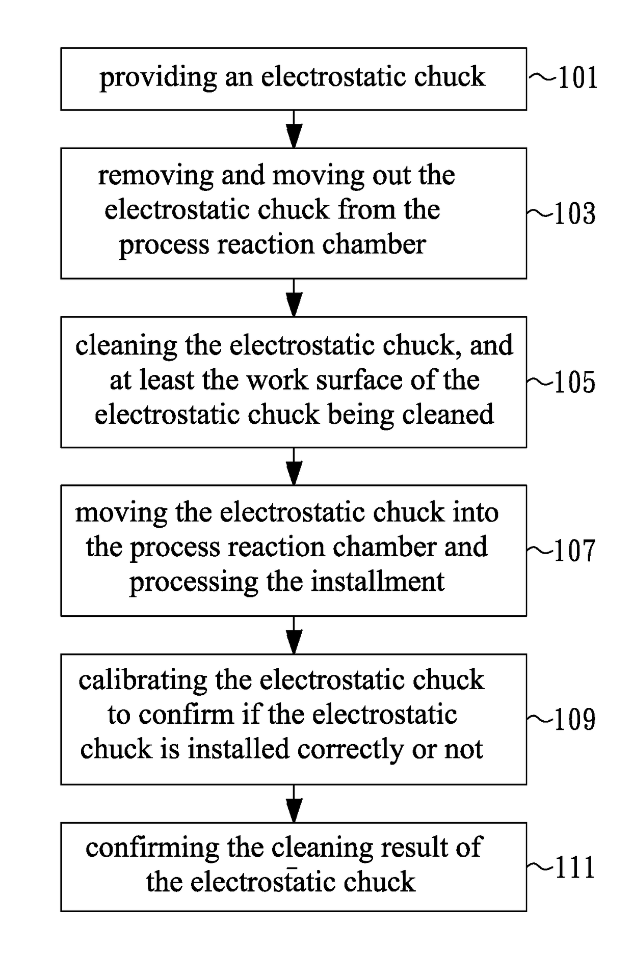
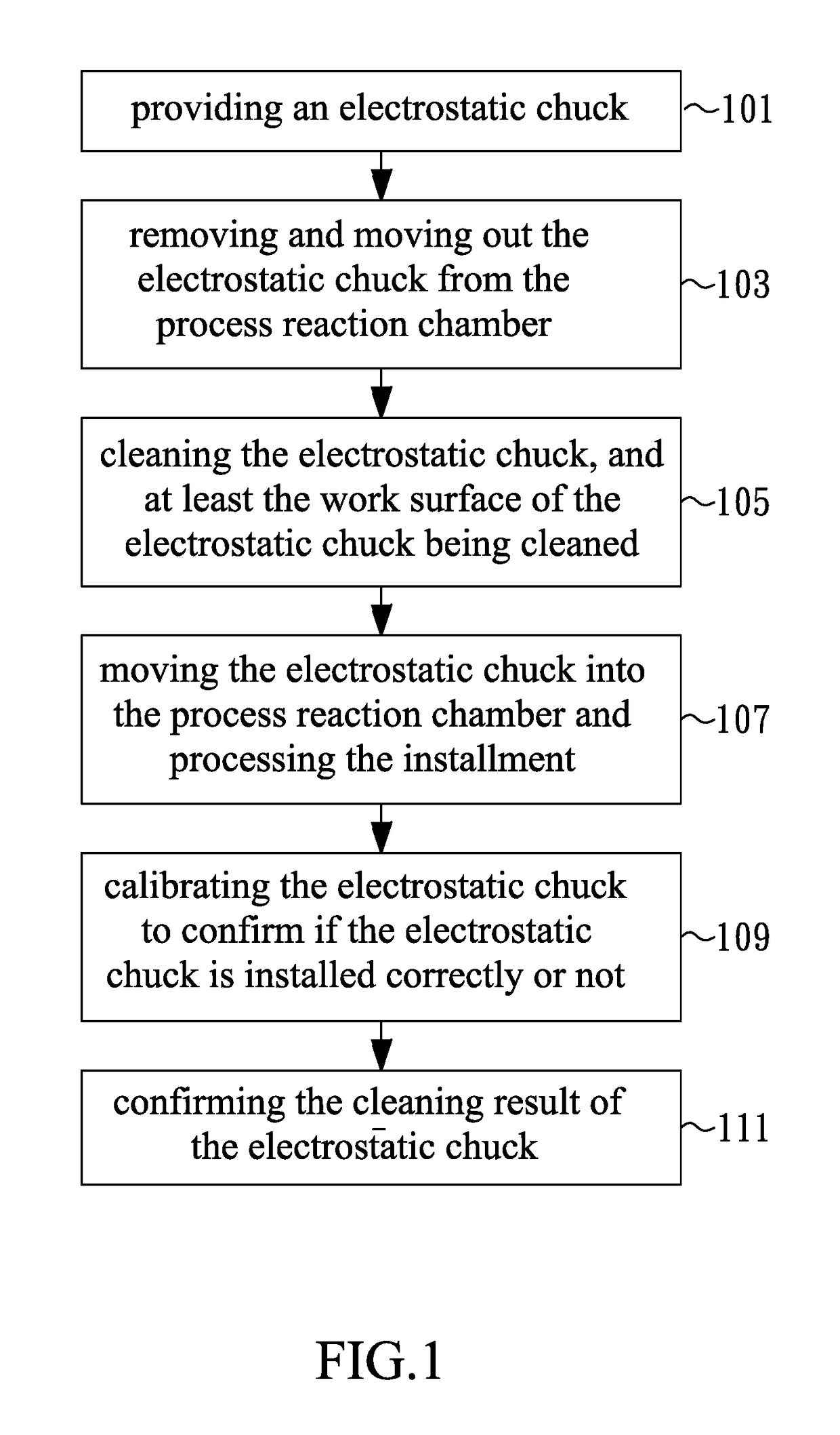
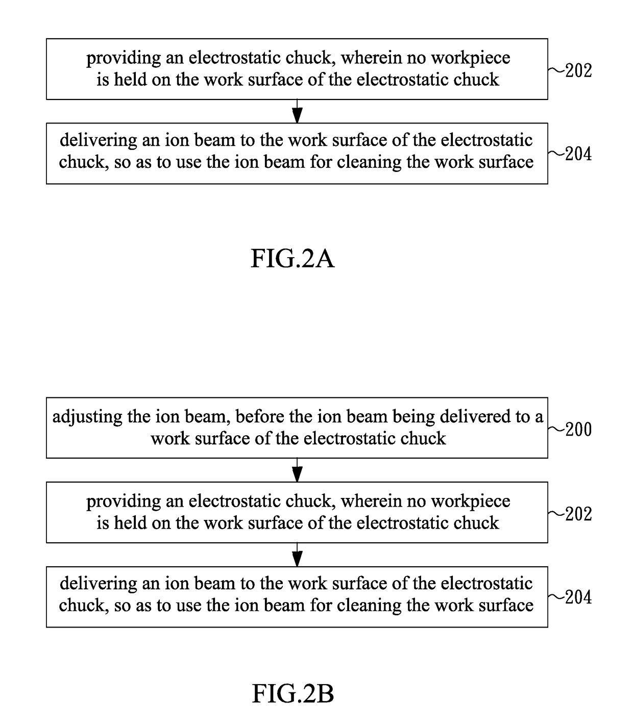
- A method involving the use of an ion beam to clean the work surface of the electrostatic chuck within the reaction chamber, adjusting the ion beam parameters based on deposition structure and material to remove contamination through physical bombardment or chemical reaction without breaking vacuum, thus avoiding hardware modifications and reducing calibration needs.

Cleaning method and method of manufacturing semiconductor device
PatentActiveUS20230173557A1
Innovation
- A cleaning method that exposes the electrostatic chuck to plasma while maintaining a potential relationship to introduce an electron current from the plasma, reducing the risk of high-energy ion collisions by using low-energy electrons for cleaning.


Environmental Impact of Plasma and Ion Beam Processes
The environmental implications of plasma and ion beam cleaning technologies for electrostatic chucks represent a critical consideration in semiconductor manufacturing sustainability. Both methods present distinct environmental profiles that significantly influence their adoption in modern fabrication facilities.
Plasma cleaning processes typically consume substantial electrical energy due to the need for generating and maintaining plasma states. The power requirements range from several kilowatts to tens of kilowatts depending on chamber size and process parameters. Additionally, plasma systems often require continuous gas flow of process gases such as oxygen, argon, or fluorine-based compounds, contributing to ongoing operational emissions and resource consumption.
Ion beam cleaning demonstrates generally lower energy consumption per cleaning cycle, as the ion generation process is more targeted and efficient. However, the vacuum requirements for ion beam systems are typically more stringent, necessitating high-performance pumping systems that consume considerable energy during operation. The process gases used in ion beam systems are often noble gases like argon, which have minimal environmental reactivity but represent ongoing material costs.
Chemical byproduct generation differs significantly between the two approaches. Plasma cleaning can produce various reactive species and potential toxic compounds, particularly when processing organic contaminants or using fluorine-based chemistries. These byproducts require careful exhaust gas treatment and scrubbing systems to prevent environmental release. Ion beam processes generally produce fewer chemical byproducts due to their primarily physical cleaning mechanism, though sputtered material removal still requires appropriate containment and disposal protocols.
Waste heat generation varies considerably between methods. Plasma systems typically generate significant thermal loads requiring active cooling systems, while ion beam processes produce more localized heating with potentially lower overall thermal management requirements. The infrastructure demands for cooling systems directly impact facility energy consumption and environmental footprint.
Long-term sustainability considerations favor ion beam technology in several aspects, including reduced chemical consumption, lower byproduct generation, and potentially extended equipment lifespans due to gentler processing conditions. However, plasma cleaning offers advantages in processing speed and throughput efficiency, which can offset environmental impacts through reduced overall processing time and facility utilization.
Plasma cleaning processes typically consume substantial electrical energy due to the need for generating and maintaining plasma states. The power requirements range from several kilowatts to tens of kilowatts depending on chamber size and process parameters. Additionally, plasma systems often require continuous gas flow of process gases such as oxygen, argon, or fluorine-based compounds, contributing to ongoing operational emissions and resource consumption.
Ion beam cleaning demonstrates generally lower energy consumption per cleaning cycle, as the ion generation process is more targeted and efficient. However, the vacuum requirements for ion beam systems are typically more stringent, necessitating high-performance pumping systems that consume considerable energy during operation. The process gases used in ion beam systems are often noble gases like argon, which have minimal environmental reactivity but represent ongoing material costs.
Chemical byproduct generation differs significantly between the two approaches. Plasma cleaning can produce various reactive species and potential toxic compounds, particularly when processing organic contaminants or using fluorine-based chemistries. These byproducts require careful exhaust gas treatment and scrubbing systems to prevent environmental release. Ion beam processes generally produce fewer chemical byproducts due to their primarily physical cleaning mechanism, though sputtered material removal still requires appropriate containment and disposal protocols.
Waste heat generation varies considerably between methods. Plasma systems typically generate significant thermal loads requiring active cooling systems, while ion beam processes produce more localized heating with potentially lower overall thermal management requirements. The infrastructure demands for cooling systems directly impact facility energy consumption and environmental footprint.
Long-term sustainability considerations favor ion beam technology in several aspects, including reduced chemical consumption, lower byproduct generation, and potentially extended equipment lifespans due to gentler processing conditions. However, plasma cleaning offers advantages in processing speed and throughput efficiency, which can offset environmental impacts through reduced overall processing time and facility utilization.
Cost-Benefit Analysis of ESC Cleaning Technologies
The economic evaluation of electrostatic chuck cleaning technologies reveals significant differences between plasma and ion beam methods across multiple cost dimensions. Initial capital expenditure represents the most substantial variance, with plasma cleaning systems typically requiring investments ranging from $200,000 to $500,000, while ion beam systems command premium pricing between $800,000 to $1.5 million due to their sophisticated beam generation and control mechanisms.
Operational expenditure patterns demonstrate contrasting profiles between the two technologies. Plasma cleaning systems exhibit higher consumable costs, primarily driven by process gas consumption, electrode replacement, and chamber component maintenance. Annual operating costs for plasma systems typically range from $50,000 to $80,000 per tool, with gas costs representing approximately 40% of total operational expenses.
Ion beam cleaning systems present lower recurring operational costs, with annual expenses typically falling between $30,000 to $50,000 per tool. The reduced consumable requirements stem from the non-contact nature of ion beam processing and minimal chamber contamination. However, these systems require specialized maintenance expertise, potentially increasing service contract costs by 20-30% compared to plasma alternatives.
Productivity analysis reveals that ion beam methods deliver superior throughput efficiency, achieving cleaning cycle times 30-50% shorter than plasma processes. This translates to enhanced wafer processing capacity and improved fab utilization rates. For high-volume manufacturing environments processing over 10,000 wafers monthly, the productivity advantage can justify the higher initial investment within 18-24 months.
Total cost of ownership calculations over a five-year operational period indicate that ion beam systems become economically favorable for facilities exceeding 8,000 wafer starts per month. Below this threshold, plasma cleaning systems maintain cost advantages despite lower individual cleaning efficiency. The break-even analysis must also incorporate yield impact considerations, as ion beam cleaning typically delivers 15-25% better particle removal efficiency, potentially reducing downstream defect rates and improving overall manufacturing economics.
Operational expenditure patterns demonstrate contrasting profiles between the two technologies. Plasma cleaning systems exhibit higher consumable costs, primarily driven by process gas consumption, electrode replacement, and chamber component maintenance. Annual operating costs for plasma systems typically range from $50,000 to $80,000 per tool, with gas costs representing approximately 40% of total operational expenses.
Ion beam cleaning systems present lower recurring operational costs, with annual expenses typically falling between $30,000 to $50,000 per tool. The reduced consumable requirements stem from the non-contact nature of ion beam processing and minimal chamber contamination. However, these systems require specialized maintenance expertise, potentially increasing service contract costs by 20-30% compared to plasma alternatives.
Productivity analysis reveals that ion beam methods deliver superior throughput efficiency, achieving cleaning cycle times 30-50% shorter than plasma processes. This translates to enhanced wafer processing capacity and improved fab utilization rates. For high-volume manufacturing environments processing over 10,000 wafers monthly, the productivity advantage can justify the higher initial investment within 18-24 months.
Total cost of ownership calculations over a five-year operational period indicate that ion beam systems become economically favorable for facilities exceeding 8,000 wafer starts per month. Below this threshold, plasma cleaning systems maintain cost advantages despite lower individual cleaning efficiency. The break-even analysis must also incorporate yield impact considerations, as ion beam cleaning typically delivers 15-25% better particle removal efficiency, potentially reducing downstream defect rates and improving overall manufacturing economics.
Unlock deeper insights with PatSnap Eureka Quick Research — get a full tech report to explore trends and direct your research. Try now!
Generate Your Research Report Instantly with AI Agent
Supercharge your innovation with PatSnap Eureka AI Agent Platform!