

Develop Synaptic Transistor Models for AI Integration
APR 17, 20269 MIN READ
Generate Your Research Report Instantly with AI Agent
Patsnap Eureka helps you evaluate technical feasibility & market potential.
Synaptic Transistor Background and AI Integration Goals
Synaptic transistors represent a revolutionary convergence of neuroscience principles and semiconductor technology, emerging as a critical component for next-generation artificial intelligence systems. These devices mimic the fundamental operations of biological synapses, enabling dynamic weight modulation and memory storage within individual transistor units. The development trajectory spans from early memristor concepts in the 1970s to contemporary neuromorphic architectures that promise to overcome the von Neumann bottleneck plaguing traditional computing systems.
The biological inspiration stems from understanding how neural synapses process and store information through variable conductance states. Synaptic transistors replicate this functionality by exhibiting controllable resistance changes in response to electrical stimuli, creating analog memory capabilities that can represent synaptic weights directly in hardware. This biomimetic approach enables massively parallel processing architectures that fundamentally differ from digital computing paradigms.
Current technological evolution focuses on various material systems including organic semiconductors, metal oxides, and two-dimensional materials such as graphene and transition metal dichalcogenides. Each material platform offers distinct advantages in terms of switching speed, retention time, energy consumption, and fabrication compatibility with existing semiconductor processes.
The primary integration goals center on developing comprehensive device models that accurately predict synaptic transistor behavior across diverse operating conditions. These models must capture essential phenomena including short-term plasticity, long-term potentiation and depression, spike-timing dependent plasticity, and multi-level conductance states. Accurate modeling enables circuit designers to implement learning algorithms directly in hardware, facilitating real-time adaptation and inference capabilities.
Key objectives include establishing standardized characterization methodologies, developing compact models suitable for circuit simulation tools, and creating scalable architectures that maintain synaptic functionality at high integration densities. The ultimate goal involves seamless integration with conventional CMOS technology to enable hybrid neuromorphic-digital systems that leverage the strengths of both computing paradigms for enhanced AI performance and energy efficiency.
Market Demand for Neuromorphic AI Computing Solutions
The neuromorphic computing market is experiencing unprecedented growth driven by the limitations of traditional von Neumann architectures in handling AI workloads efficiently. Current computing systems face significant challenges in power consumption and processing speed when executing complex neural network operations, creating substantial demand for brain-inspired computing solutions that can process information more naturally and efficiently.
Edge computing applications represent a primary driver for neuromorphic AI solutions, particularly in Internet of Things devices, autonomous vehicles, and mobile platforms where power efficiency is critical. These applications require real-time processing capabilities with minimal energy consumption, making synaptic transistor-based systems highly attractive for manufacturers seeking competitive advantages in battery-powered devices.
The healthcare and biomedical sectors demonstrate strong demand for neuromorphic computing solutions, especially in medical imaging, diagnostic systems, and prosthetic devices. Brain-computer interfaces and neural implants require computing architectures that can seamlessly integrate with biological neural networks, positioning synaptic transistor models as essential components for next-generation medical technologies.
Industrial automation and robotics markets are increasingly seeking neuromorphic solutions for adaptive control systems, pattern recognition, and sensory processing applications. Manufacturing companies require AI systems capable of learning and adapting to changing environments without extensive reprogramming, driving demand for hardware that can implement synaptic plasticity and learning algorithms directly at the device level.
The defense and aerospace industries present significant market opportunities for neuromorphic computing, particularly in autonomous systems, surveillance technologies, and signal processing applications. These sectors require robust, low-power computing solutions capable of operating in challenging environments while maintaining high performance standards.
Consumer electronics manufacturers are exploring neuromorphic integration for smart devices, wearable technology, and home automation systems. The growing demand for always-on AI capabilities in smartphones, smart speakers, and other connected devices creates substantial market potential for synaptic transistor-based solutions that can provide continuous learning and adaptation without draining battery resources.
Research institutions and academic organizations constitute an important market segment, driving demand for neuromorphic computing platforms for scientific research, algorithm development, and educational purposes. This segment influences long-term market trends and technological advancement directions.
Current State and Challenges of Synaptic Transistor Technology
Synaptic transistor technology has emerged as a promising neuromorphic computing paradigm that mimics biological neural networks by integrating memory and processing functions within individual devices. Current implementations primarily utilize memristive materials, organic semiconductors, and ion-gated transistors to achieve synaptic plasticity. These devices demonstrate fundamental synaptic behaviors including short-term and long-term potentiation, spike-timing-dependent plasticity, and paired-pulse facilitation.
The geographical distribution of synaptic transistor research shows concentrated efforts in East Asia, particularly South Korea, China, and Japan, with significant contributions from North American and European institutions. Leading research centers have developed various material platforms including oxide-based memristors, organic electrochemical transistors, and two-dimensional material systems. Manufacturing capabilities remain largely confined to specialized research facilities and select semiconductor foundries with advanced process nodes.
Despite substantial progress, several critical challenges impede widespread adoption of synaptic transistor technology. Device variability represents a fundamental obstacle, as manufacturing tolerances significantly impact synaptic weight precision and network reliability. Current fabrication processes struggle to achieve the uniformity required for large-scale neural network implementations, with device-to-device variations often exceeding acceptable thresholds for practical AI applications.
Endurance limitations pose another significant constraint, as repeated programming cycles degrade synaptic functionality over time. Most current devices demonstrate limited cycling endurance compared to conventional memory technologies, restricting their applicability in continuous learning scenarios. Additionally, power consumption remains elevated compared to biological synapses, particularly during weight update operations.
Integration complexity presents substantial engineering challenges, as synaptic transistors require specialized peripheral circuits for programming, reading, and control operations. Current architectures lack standardized interfaces and suffer from limited scalability when transitioning from laboratory demonstrations to commercial implementations. The absence of mature design automation tools further complicates system-level integration efforts.
Temperature sensitivity and environmental stability issues affect device performance consistency across operational conditions. Many synaptic transistor implementations exhibit significant parameter drift under thermal stress or humidity variations, compromising long-term reliability. Furthermore, the lack of comprehensive reliability models hampers accurate prediction of device behavior in real-world deployment scenarios.
Existing Synaptic Transistor Models and Implementations
01 Neuromorphic computing architectures using synaptic transistors
Synaptic transistor models are implemented in neuromorphic computing systems that mimic biological neural networks. These architectures utilize transistor devices that can emulate synaptic behavior, including weight adjustment and learning mechanisms. The models enable parallel processing and low-power computation by replicating the functionality of biological synapses through electronic components. These systems can perform pattern recognition, associative learning, and other cognitive tasks through hardware-based neural network implementations.- Neuromorphic computing architectures using synaptic transistors: Synaptic transistor models are implemented in neuromorphic computing systems that mimic biological neural networks. These architectures utilize transistor devices that can emulate synaptic behavior, including weight adjustment and learning mechanisms. The models enable parallel processing and low-power computation by replicating the plasticity and connectivity patterns found in biological synapses. Such systems are designed for artificial intelligence applications, pattern recognition, and cognitive computing tasks.
- Memristive and resistive switching devices for synaptic modeling: Synaptic transistor models incorporate memristive or resistive switching elements that can change their conductance states to represent synaptic weights. These devices exhibit analog memory characteristics that allow gradual modulation of conductance, mimicking the strengthening or weakening of synaptic connections. The resistance states can be programmed through electrical pulses, enabling implementation of spike-timing-dependent plasticity and other learning rules essential for neural network training.
- Three-terminal synaptic transistor structures: Three-terminal transistor configurations are employed to create synaptic devices with enhanced control over synaptic operations. These structures typically include gate, source, and drain terminals that allow independent control of reading and writing operations. The gate terminal can modulate the channel conductance to simulate synaptic weight changes, while the source-drain current represents the synaptic signal transmission. Such architectures provide better separation between learning and inference operations.
- Organic and flexible materials for synaptic transistors: Synaptic transistor models utilize organic semiconductors and flexible substrate materials to create biocompatible and mechanically adaptable devices. These materials enable the fabrication of synaptic transistors that can interface with biological systems or be integrated into wearable electronics. The organic materials exhibit ion migration and charge trapping properties that naturally emulate synaptic plasticity mechanisms, providing advantages for low-voltage operation and solution-based processing.
- Multi-level conductance states and analog computing: Synaptic transistor models are designed to achieve multiple discrete or continuous conductance levels that represent different synaptic weight values. These multi-level states enable analog computation within neural networks, reducing the need for digital conversion and improving energy efficiency. Programming schemes are developed to precisely control and maintain these conductance states over time, addressing challenges such as state drift and variability. The analog nature of these devices allows for more efficient implementation of multiply-accumulate operations fundamental to neural network processing.
02 Memristive and resistive switching devices for synaptic modeling
Synaptic transistor models incorporate memristive elements and resistive switching mechanisms to achieve analog weight storage and synaptic plasticity. These devices exhibit conductance changes in response to electrical stimuli, mimicking the strengthening or weakening of synaptic connections. The resistance states can be programmed to represent synaptic weights, enabling non-volatile memory characteristics. Multiple resistance levels allow for multi-bit storage and gradual learning processes similar to biological long-term potentiation and depression.Expand Specific Solutions03 Three-terminal synaptic transistor structures
Three-terminal transistor configurations are employed to model synaptic functions with enhanced control capabilities. These structures typically include gate, source, and drain terminals that allow independent control of synaptic weight and signal transmission. The gate terminal can modulate the conductance between source and drain, simulating the role of neurotransmitters in biological synapses. Such configurations enable both excitatory and inhibitory synaptic behaviors and support spike-timing-dependent plasticity mechanisms.Expand Specific Solutions04 Organic and nanomaterial-based synaptic transistors
Synaptic transistor models utilize organic semiconductors and nanomaterials to achieve flexible, biocompatible, and scalable implementations. These materials enable the fabrication of transistors with tunable electrical properties that can emulate various synaptic characteristics. Nanostructured channels and interfaces provide enhanced surface-to-volume ratios for improved sensitivity and response times. The use of novel materials allows for low-voltage operation and integration with biological systems for neuromorphic applications.Expand Specific Solutions05 Circuit modeling and simulation frameworks for synaptic transistors
Comprehensive circuit models and simulation frameworks are developed to characterize and predict the behavior of synaptic transistors in neural network applications. These models incorporate electrical parameters, temporal dynamics, and plasticity rules to accurately represent synaptic operations. Simulation tools enable the design and optimization of large-scale neuromorphic systems before physical implementation. The frameworks support various learning algorithms and network topologies, facilitating the development of efficient hardware neural networks.Expand Specific Solutions
Key Players in Synaptic Device and Neuromorphic Industry
The synaptic transistor technology for AI integration represents an emerging field in the early development stage, with significant growth potential driven by the convergence of neuromorphic computing and artificial intelligence demands. The market remains nascent but shows promising expansion as organizations seek brain-inspired computing solutions for energy-efficient AI processing. Technology maturity varies considerably across participants, with established semiconductor leaders like Intel Corp., Samsung Electronics, Taiwan Semiconductor Manufacturing, and IBM demonstrating advanced capabilities in neuromorphic device development. Academic institutions including KAIST, Peking University, and various Chinese universities contribute fundamental research breakthroughs, while specialized companies like MediaTek and Texas Instruments explore commercial applications. The competitive landscape features a hybrid ecosystem where traditional chip manufacturers collaborate with research institutions to accelerate development, though most implementations remain in prototype or early commercialization phases, indicating substantial room for technological advancement and market penetration.
Intel Corp.
Technical Solution: Intel has developed neuromorphic computing architectures that incorporate synaptic transistor models for AI integration. Their Loihi neuromorphic processor utilizes artificial synapses that can adapt their connection strengths through spike-timing-dependent plasticity mechanisms. The synaptic transistors in their design feature programmable conductance states that mimic biological synaptic behavior, enabling real-time learning and adaptation. Intel's approach focuses on creating energy-efficient synaptic devices that can perform both memory and computation functions simultaneously, reducing the von Neumann bottleneck. Their synaptic transistor models incorporate multi-level conductance states and temporal dynamics that closely resemble biological neural networks, making them suitable for edge AI applications requiring low power consumption and real-time processing capabilities.
Strengths: Established neuromorphic computing platform with proven synaptic transistor implementations, strong industry partnerships for commercialization. Weaknesses: Limited scalability compared to traditional CMOS processes, higher manufacturing costs for specialized neuromorphic chips.
Taiwan Semiconductor Manufacturing Co., Ltd.
Technical Solution: TSMC has developed specialized process technologies for manufacturing synaptic transistors used in neuromorphic computing and AI integration applications. Their approach focuses on creating CMOS-compatible synaptic devices that can be integrated with conventional digital circuits on the same chip. TSMC's synaptic transistor models utilize floating-gate and charge-trap mechanisms to achieve programmable conductance states that mimic biological synaptic behavior. The company has demonstrated synaptic devices with precise conductance control, low power operation, and excellent retention characteristics. Their manufacturing process enables the creation of dense synaptic arrays with high uniformity and yield, essential for large-scale neural network implementations. TSMC's synaptic transistor technology supports both volatile and non-volatile operation modes, allowing for flexible implementation of different neural network architectures and learning algorithms in AI systems.
Strengths: World-class semiconductor manufacturing capabilities, CMOS compatibility for easy integration, high yield and uniformity in large-scale production. Weaknesses: Primarily a foundry service provider rather than system integrator, limited direct involvement in AI algorithm development, dependency on customer designs for optimization.
Core Innovations in Synaptic Plasticity Modeling
Synaptic transistor and method for manufacturing the same
PatentActiveKR1020220032688A
Innovation
- A synaptic transistor with a substrate, bottom gate electrode, floating gate electrode, and ion-containing gate insulating layers, utilizing hydrogen ions for short-term memory and charge traps for long-term memory, achieved through a combination of gate biases and FN tunneling mechanisms.


Synaptic transistor based on metal nano-sheet and method of manufacturing the same
PatentActiveUS20180083212A1
Innovation
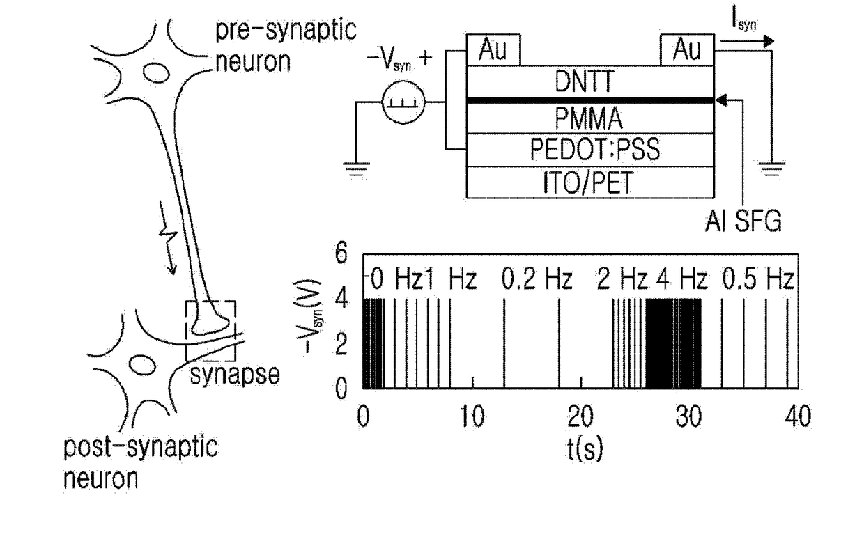
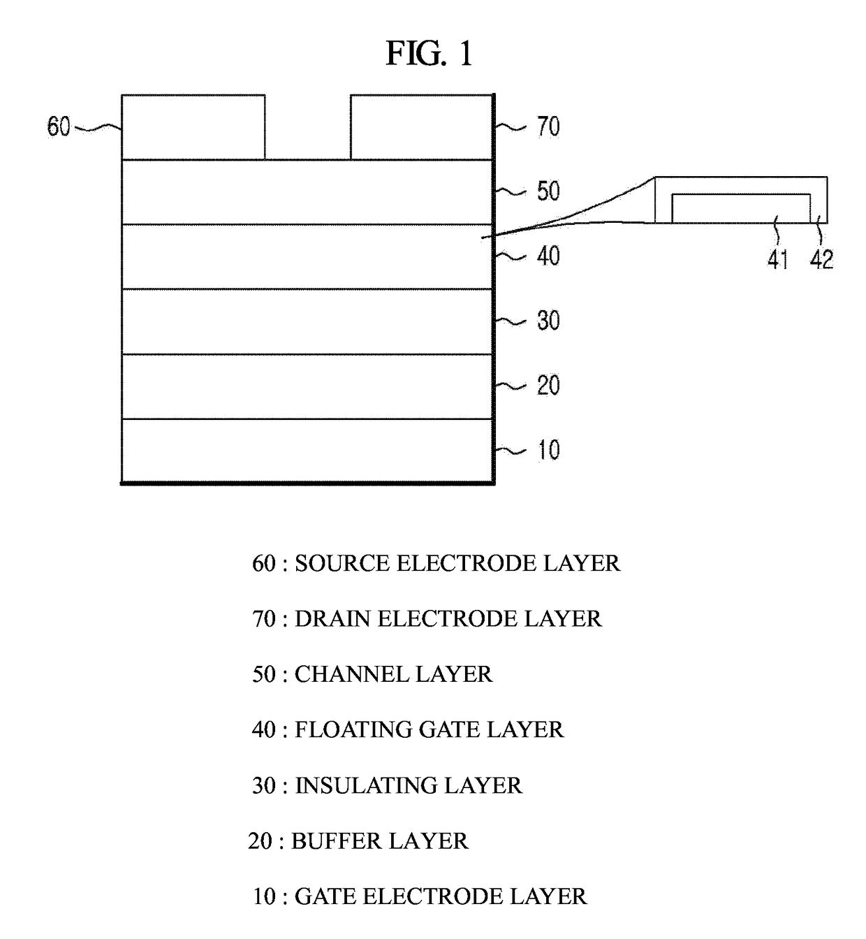
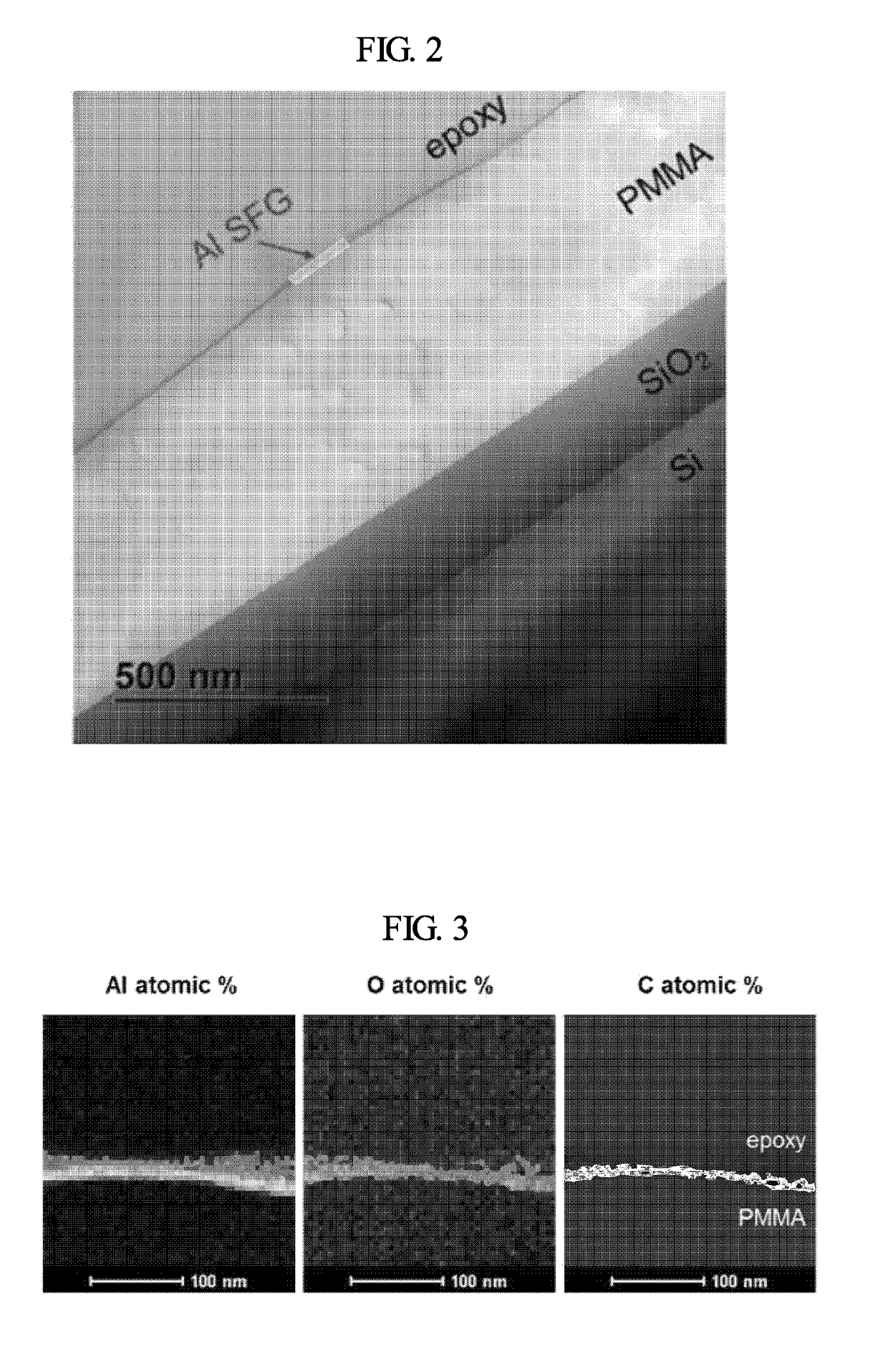
- A synaptic transistor based on a metal nano-sheet structure, featuring a gate electrode layer, buffer layer, insulating layer, self-assembled floating gate layer, source electrode layer, and drain electrode layer, where the self-assembled floating gate layer includes naturally oxidizing materials like silver, copper, or aluminum, and a metal oxide layer for efficient charge storage and isolation.

Hardware-Software Co-design for Neuromorphic Systems
The development of effective synaptic transistor models for AI integration necessitates a comprehensive hardware-software co-design approach that bridges the gap between neuromorphic hardware capabilities and AI algorithm requirements. This interdisciplinary methodology ensures optimal performance by simultaneously optimizing both hardware architecture and software implementation strategies.
At the hardware level, synaptic transistor models must accurately capture the complex dynamics of biological synapses while maintaining computational efficiency. The co-design process involves developing device-level models that can be seamlessly integrated into circuit simulators and system-level design tools. These models must account for device variability, non-linear behavior, and temporal dynamics that are characteristic of synaptic operations.
Software frameworks play a crucial role in translating high-level AI algorithms into neuromorphic implementations. The co-design approach requires developing specialized compilers and mapping tools that can efficiently partition neural network computations across arrays of synaptic transistors. These tools must consider hardware constraints such as limited precision, device mismatch, and energy consumption while preserving algorithm accuracy.
The integration process involves creating abstraction layers that enable seamless communication between software models and hardware implementations. This includes developing standardized interfaces for synaptic parameter programming, weight update protocols, and spike-timing dependent plasticity mechanisms. The abstraction layers must provide sufficient flexibility to support various AI algorithms while maintaining hardware efficiency.
Cross-layer optimization represents a key advantage of the co-design methodology. By jointly optimizing hardware parameters and software algorithms, designers can achieve superior performance compared to traditional sequential design approaches. This includes optimizing synaptic weight encoding schemes, developing fault-tolerant algorithms that can handle device variations, and implementing adaptive calibration mechanisms.
Validation and verification frameworks are essential components of the co-design process. These frameworks must enable comprehensive testing of synaptic transistor models across different abstraction levels, from device physics to system-level AI applications. The validation process ensures that hardware-software interactions meet performance specifications and maintain algorithmic fidelity throughout the design hierarchy.
Energy Efficiency Standards for Brain-Inspired Computing
The development of energy efficiency standards for brain-inspired computing represents a critical milestone in establishing sustainable neuromorphic systems. Current industry initiatives focus on defining power consumption benchmarks that mirror biological neural networks, where synaptic operations consume minimal energy compared to traditional digital processors. These standards aim to establish maximum power density thresholds of 10-20 watts per square centimeter for neuromorphic chips, significantly lower than conventional processors.
Emerging standardization efforts concentrate on dynamic power scaling mechanisms that adapt energy consumption based on computational workload. Brain-inspired systems demonstrate inherent advantages through event-driven processing, where synaptic transistors activate only when receiving input signals, dramatically reducing idle power consumption. This approach contrasts sharply with traditional computing architectures that maintain constant power draw regardless of processing demands.
International organizations are developing comprehensive evaluation frameworks that assess energy efficiency across multiple operational scenarios. These frameworks incorporate metrics such as operations per joule, standby power consumption, and thermal management capabilities. The standards emphasize the importance of measuring energy efficiency during both training and inference phases of AI applications, recognizing that neuromorphic systems exhibit different power profiles across these operational modes.
Regulatory bodies are establishing certification processes that validate compliance with energy efficiency requirements for brain-inspired computing systems. These certifications consider factors including manufacturing process variations, temperature dependencies, and long-term reliability impacts on power consumption. The standards also address scalability concerns, ensuring that energy efficiency metrics remain consistent as neuromorphic systems expand from laboratory prototypes to commercial deployments.
Future standardization roadmaps anticipate incorporating adaptive efficiency targets that evolve with technological advancement. These dynamic standards will accommodate emerging materials and device architectures while maintaining stringent energy consumption limits. The integration of machine learning algorithms for power optimization within the standards framework represents a novel approach to achieving sustained energy efficiency improvements in brain-inspired computing platforms.
Unlock deeper insights with Patsnap Eureka Quick Research — get a full tech report to explore trends and direct your research. Try now!
Generate Your Research Report Instantly with AI Agent
Supercharge your innovation with Patsnap Eureka AI Agent Platform!