

Signal Integrity in Synaptic Transistor Implementations
APR 17, 20269 MIN READ
Generate Your Research Report Instantly with AI Agent
Patsnap Eureka helps you evaluate technical feasibility & market potential.
Synaptic Transistor Signal Integrity Background and Objectives
Synaptic transistors represent a revolutionary paradigm in neuromorphic computing, emerging from the convergence of neuroscience principles and semiconductor technology. These devices aim to emulate the fundamental operations of biological synapses through electronic implementations, enabling brain-inspired computing architectures that can process information with unprecedented efficiency and adaptability.
The evolution of synaptic transistors traces back to early memristor research in the 2000s, where scientists first demonstrated the possibility of creating electronic devices with memory-dependent conductance properties. This foundational work paved the way for more sophisticated implementations that could mimic synaptic plasticity, the cornerstone of learning and memory in biological neural networks.
Signal integrity emerges as a critical challenge in synaptic transistor implementations due to the unique operational requirements of these devices. Unlike conventional digital transistors that operate in binary states, synaptic transistors must maintain precise analog conductance levels that represent synaptic weights. These analog states are susceptible to various forms of signal degradation, including noise interference, crosstalk between adjacent devices, and temporal drift phenomena.
The primary technical objectives center on achieving reliable signal transmission and preservation of synaptic weight information across large-scale neuromorphic arrays. This involves maintaining consistent conductance modulation characteristics, minimizing unwanted signal variations, and ensuring stable long-term retention of programmed states. Additionally, the implementation must support high-frequency operation while preserving the fidelity of spike-timing dependent plasticity mechanisms.
Current research efforts focus on developing robust signaling protocols that can accommodate the inherent variability of synaptic devices while maintaining computational accuracy. This includes investigating advanced error correction schemes, optimized array architectures, and novel materials that exhibit improved signal stability characteristics.
The ultimate goal is to establish comprehensive design methodologies that enable the deployment of large-scale synaptic transistor networks with predictable and reliable signal integrity performance, thereby unlocking the full potential of neuromorphic computing systems for applications ranging from artificial intelligence to autonomous robotics.
Market Demand for Neuromorphic Computing Solutions
The neuromorphic computing market is experiencing unprecedented growth driven by the increasing demand for energy-efficient artificial intelligence solutions across multiple industries. Traditional von Neumann architectures face significant limitations in handling the massive parallel processing requirements of modern AI applications, creating substantial market opportunities for brain-inspired computing paradigms. The convergence of edge computing demands, Internet of Things proliferation, and autonomous system requirements has established neuromorphic solutions as critical enablers for next-generation intelligent systems.
Healthcare and medical device sectors represent one of the most promising application domains for neuromorphic computing solutions. Neural prosthetics, brain-computer interfaces, and real-time medical monitoring systems require ultra-low power consumption and real-time processing capabilities that align perfectly with synaptic transistor implementations. The ability to process sensory data with minimal latency while maintaining extended battery life makes neuromorphic architectures particularly attractive for implantable medical devices and wearable health monitoring systems.
Autonomous vehicle development has created substantial demand for neuromorphic computing solutions capable of real-time sensor fusion and decision-making processes. The automotive industry requires computing systems that can process multiple data streams from cameras, lidar, and radar sensors simultaneously while maintaining strict power and thermal constraints. Synaptic transistor implementations offer the potential for distributed processing architectures that can handle complex pattern recognition tasks with significantly reduced energy consumption compared to traditional digital processors.
Industrial automation and robotics applications are driving increased adoption of neuromorphic computing solutions for adaptive control systems and predictive maintenance applications. Manufacturing environments require intelligent systems capable of learning from operational data and adapting to changing conditions without extensive reprogramming. The inherent learning capabilities of synaptic transistor networks make them ideal for applications requiring continuous adaptation and optimization in dynamic industrial environments.
Consumer electronics manufacturers are increasingly exploring neuromorphic computing solutions for next-generation smartphones, smart home devices, and augmented reality systems. The demand for always-on artificial intelligence capabilities while maintaining acceptable battery life has created significant market pressure for energy-efficient computing architectures. Synaptic transistor implementations promise to enable sophisticated AI functionality in portable devices without the thermal and power limitations associated with traditional digital processing approaches.
The defense and aerospace sectors represent emerging high-value markets for neuromorphic computing solutions, particularly for autonomous systems operating in resource-constrained environments. Space applications, unmanned aerial vehicles, and battlefield intelligence systems require robust computing architectures capable of operating reliably under extreme conditions while maintaining minimal power consumption profiles.
Current Signal Integrity Challenges in Synaptic Devices
Synaptic transistor implementations face significant signal integrity challenges that fundamentally limit their performance in neuromorphic computing applications. The primary issue stems from the inherent variability in conductance modulation, where synaptic weights cannot be precisely controlled due to stochastic switching mechanisms in memristive materials. This variability manifests as device-to-device variations exceeding 20% in many implementations, creating substantial noise floors that compromise computational accuracy.
Temporal signal degradation represents another critical challenge, particularly in analog synaptic devices where charge leakage and drift phenomena cause gradual weight decay. The retention characteristics of synaptic states typically exhibit exponential decay with time constants ranging from seconds to hours, depending on the underlying physical mechanisms. This temporal instability directly impacts the reliability of stored synaptic weights and necessitates frequent refresh operations that increase power consumption.
Crosstalk interference between adjacent synaptic elements poses severe constraints on array scalability. In dense crossbar architectures, parasitic current paths through neighboring devices create sneak currents that distort intended synaptic operations. The magnitude of this interference scales quadratically with array size, making large-scale implementations increasingly problematic. Current mitigation strategies involving selector devices introduce additional complexity and area overhead.
Non-linear switching dynamics in synaptic transistors create asymmetric potentiation and depression characteristics that complicate learning algorithm implementation. The switching kinetics often exhibit threshold-dependent behavior with different time constants for positive and negative weight updates. This asymmetry leads to systematic biases in synaptic plasticity that can degrade learning performance and require algorithmic compensation.
Process variations during fabrication introduce systematic and random variations in device parameters that affect signal integrity across entire arrays. Critical parameters such as threshold voltages, switching ratios, and retention characteristics show significant statistical distributions that impact yield and uniformity. These variations are particularly pronounced in emerging materials and novel device structures where manufacturing processes are not yet mature.
Thermal effects present additional signal integrity challenges, as elevated temperatures accelerate drift mechanisms and alter switching characteristics. The temperature dependence of synaptic operations creates stability issues in practical implementations where thermal management becomes crucial for maintaining signal fidelity across varying operating conditions.
Existing Signal Integrity Enhancement Solutions
01 Synaptic transistor circuit design and architecture
Synaptic transistors can be designed with specific circuit architectures to improve signal integrity. This includes optimizing the transistor structure, gate configurations, and interconnection schemes to minimize signal degradation and noise. Advanced circuit topologies can enhance the reliability of signal transmission in neuromorphic computing systems by reducing parasitic effects and improving signal-to-noise ratios.- Synaptic transistor circuit design and architecture: Synaptic transistors can be designed with specific circuit architectures to improve signal integrity. This includes optimizing the transistor structure, gate configurations, and interconnection schemes to minimize signal degradation and noise. Advanced circuit topologies can enhance the reliability of signal transmission in neuromorphic computing systems by reducing parasitic effects and improving signal-to-noise ratios.
- Signal processing and conditioning techniques: Various signal processing methods can be employed to maintain signal integrity in synaptic transistor systems. These techniques include signal amplification, filtering, and compensation circuits that correct for signal distortions. By implementing appropriate signal conditioning stages, the fidelity of neural signals can be preserved throughout the transmission path, ensuring accurate synaptic weight updates and neural network operations.
- Material selection and device fabrication for improved signal characteristics: The choice of materials and fabrication processes significantly impacts signal integrity in synaptic transistors. Advanced materials with superior electrical properties can reduce signal attenuation and improve switching characteristics. Specialized fabrication techniques can create devices with enhanced performance metrics, including faster response times, lower power consumption, and reduced signal interference.
- Noise reduction and interference mitigation strategies: Implementing noise reduction techniques is crucial for maintaining signal integrity in synaptic transistor arrays. This includes shielding strategies, ground plane optimization, and isolation techniques that minimize crosstalk between adjacent devices. Advanced layout designs and electromagnetic interference suppression methods can significantly improve the overall signal quality in dense neuromorphic circuits.
- Timing and synchronization control mechanisms: Precise timing control and synchronization are essential for preserving signal integrity in synaptic transistor networks. This involves implementing clock distribution networks, delay compensation circuits, and synchronization protocols that ensure coordinated signal transmission across multiple synaptic elements. Proper timing management prevents signal skew and maintains the temporal relationships critical for neural network functionality.
02 Signal processing and conditioning techniques
Various signal processing methods can be employed to maintain signal integrity in synaptic transistor systems. These techniques include signal amplification, filtering, and error correction mechanisms that compensate for signal attenuation and distortion. Implementation of adaptive signal conditioning circuits helps preserve the fidelity of neural signals during transmission and processing stages.Expand Specific Solutions03 Material selection and device fabrication
The choice of materials and fabrication processes significantly impacts signal integrity in synaptic transistors. Utilizing high-quality semiconductor materials, optimized dielectric layers, and advanced deposition techniques can reduce interface defects and improve electrical characteristics. Proper material engineering enhances device performance by minimizing leakage currents and improving switching characteristics.Expand Specific Solutions04 Noise reduction and shielding strategies
Implementing effective noise reduction and electromagnetic shielding techniques is crucial for maintaining signal integrity. This includes the use of guard rings, isolation structures, and proper grounding schemes to minimize crosstalk and external interference. Shielding strategies help protect sensitive synaptic signals from electromagnetic interference and substrate noise in integrated circuits.Expand Specific Solutions05 Timing control and synchronization mechanisms
Precise timing control and synchronization are essential for preserving signal integrity in synaptic transistor networks. This involves implementing clock distribution networks, delay compensation circuits, and synchronization protocols that ensure accurate signal timing across multiple synaptic elements. Proper timing management prevents signal skew and maintains the temporal precision required for neuromorphic computing applications.Expand Specific Solutions
Key Players in Neuromorphic and Synaptic Device Industry
The signal integrity in synaptic transistor implementations represents an emerging neuromorphic computing field currently in its early development stage, with significant market potential driven by AI and edge computing demands. The technology maturity varies considerably across key players, with established semiconductor giants like Samsung Electronics, Intel, TSMC, and NVIDIA leading advanced research and manufacturing capabilities. Companies such as IBM and Toshiba contribute foundational research, while specialized firms like Lattice Semiconductor focus on programmable logic solutions. Academic institutions including KAIST, Shanghai University, and Tongji University provide crucial theoretical foundations. The competitive landscape shows a mix of memory specialists like SK Hynix developing synaptic devices, EDA companies like Cadence providing design tools, and emerging players exploring novel approaches, indicating a fragmented but rapidly evolving market with substantial growth opportunities.
Samsung Electronics Co., Ltd.
Technical Solution: Samsung has pioneered synaptic transistor implementations using phase-change memory (PCM) and resistive RAM (ReRAM) technologies with enhanced signal integrity through innovative device engineering. Their approach focuses on reducing programming noise and improving retention characteristics by optimizing material compositions and device geometries. Samsung's synaptic devices feature multi-bit storage capabilities with precise conductance control, implementing advanced read/write circuits that minimize signal distortion during synaptic operations. The company has demonstrated crossbar array architectures with effective sneak path suppression and improved signal-to-noise ratios for reliable neural network inference and training applications.
Strengths: Leading memory technology expertise, strong manufacturing capabilities, comprehensive device characterization. Weaknesses: Scalability challenges in large arrays, power consumption concerns, limited software ecosystem for neuromorphic applications.
International Business Machines Corp.
Technical Solution: IBM has pioneered synaptic transistor research through their neuromorphic computing initiatives, developing phase-change memory synapses with exceptional signal integrity characteristics. Their approach utilizes crystalline-amorphous phase transitions in chalcogenide materials to achieve precise synaptic weight control with minimal signal degradation. IBM's TrueNorth chip architecture demonstrates effective signal integrity management through event-driven communication protocols and distributed processing that reduces signal interference. The company has implemented advanced calibration techniques and compensation algorithms to maintain signal fidelity across temperature variations and aging effects, incorporating machine learning-based adaptation mechanisms for long-term stability in synaptic operations.
Strengths: Strong research foundation, innovative neuromorphic architectures, comprehensive system-level approach. Weaknesses: Limited commercial scalability, high research and development costs, complex integration requirements for practical applications.
Core Innovations in Synaptic Signal Processing
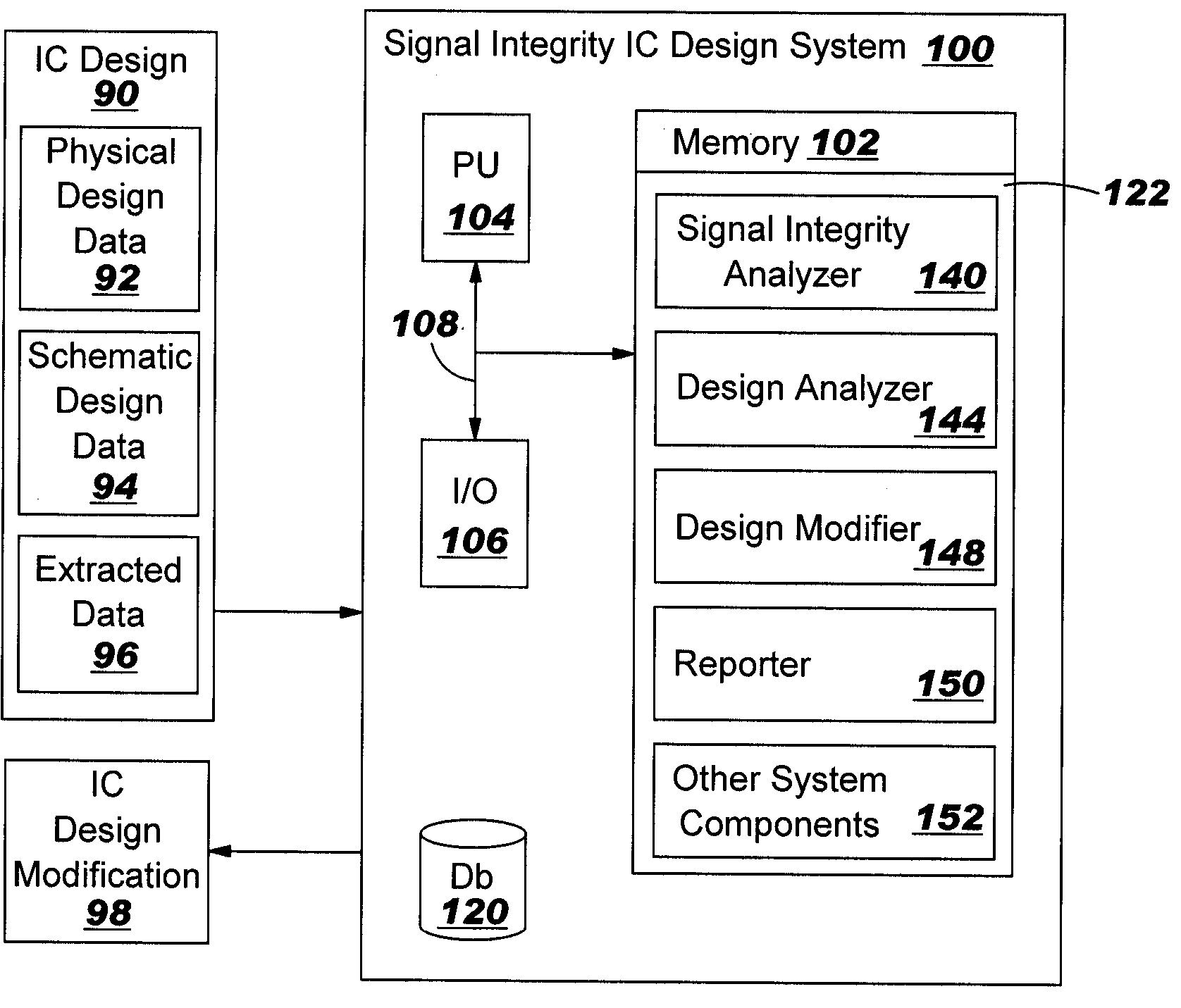
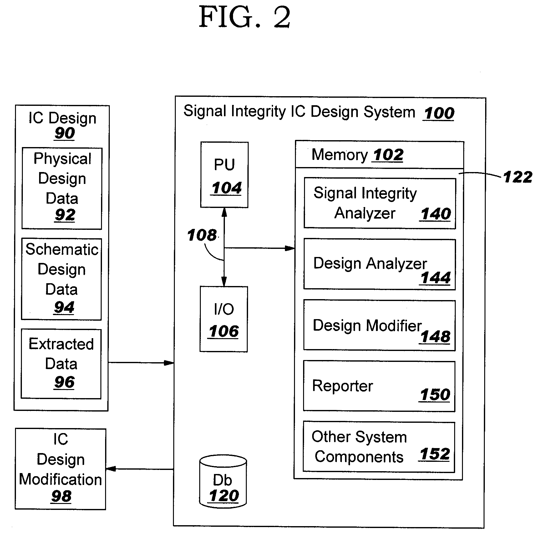
Integrated circuit design for signal integrity, avoiding well proximity effects
PatentInactiveUS20050210431A1
Innovation
- A system and method that automates the identification and modification of field effect transistors (FETs) closer than a threshold distance to a well edge, using a signal integrity analysis tool to determine failing FETs and automatically adjusting their edges to improve signal integrity, eliminating the need for manual iteration.

Synaptic transistor
PatentPendingUS20250056845A1
Innovation
- A synaptic transistor design that incorporates a substrate, an expansion gate electrode, a gate insulating layer with ions, a channel layer, source and drain electrodes, and a pad electrode, which allows for the movement of hydrogen ions to adjust the threshold voltage and enhance synaptic characteristics, including short-term and long-term memory capabilities.


Manufacturing Standards for Neuromorphic Devices
The establishment of comprehensive manufacturing standards for neuromorphic devices represents a critical foundation for ensuring reliable signal integrity in synaptic transistor implementations. Current industry efforts focus on developing standardized fabrication protocols that address the unique requirements of neuromorphic computing architectures, where precise control over device variability and performance consistency directly impacts synaptic functionality.
Material specification standards have emerged as a primary concern, particularly for memristive and phase-change materials used in synaptic transistors. These standards define acceptable ranges for material composition, crystalline structure, and electrical properties that ensure consistent switching behavior and retention characteristics. The International Electrotechnical Commission and IEEE have initiated working groups to establish baseline requirements for neuromorphic device materials, addressing issues such as endurance cycling, temperature stability, and aging effects that significantly influence signal integrity.
Process control standards encompass critical manufacturing parameters including deposition techniques, annealing procedures, and lithographic precision requirements. These specifications ensure that synaptic transistors maintain uniform electrical characteristics across wafer-scale production, minimizing device-to-device variations that could compromise network-level signal processing accuracy. Advanced process monitoring techniques, including in-situ electrical characterization and real-time feedback control systems, are being standardized to maintain tight tolerances during fabrication.
Quality assurance frameworks specifically tailored for neuromorphic devices incorporate multi-level testing protocols that evaluate both individual device performance and array-level functionality. These standards define acceptable ranges for key parameters such as conductance modulation linearity, switching speed uniformity, and noise characteristics that directly affect synaptic signal transmission fidelity.
Packaging and interconnect standards address the unique challenges of neuromorphic device integration, including thermal management requirements and electromagnetic interference mitigation strategies. These specifications ensure that signal integrity is preserved throughout the complete system implementation, from individual synaptic elements to large-scale neuromorphic arrays, establishing a foundation for reliable and scalable neuromorphic computing platforms.
Power Efficiency Considerations in Synaptic Arrays
Power consumption represents a critical design constraint in synaptic array architectures, directly impacting the scalability and practical deployment of neuromorphic computing systems. The energy efficiency of synaptic transistor implementations fundamentally determines the feasibility of large-scale neural network emulation, where millions of synaptic connections must operate simultaneously within reasonable power budgets.
Static power dissipation emerges as a primary concern in synaptic arrays, particularly when utilizing conventional CMOS-based implementations. Leakage currents through synaptic transistors accumulate across massive arrays, creating substantial baseline power consumption even during idle states. This challenge becomes exponentially more severe as array dimensions increase, potentially limiting the maximum achievable network size within given thermal and power constraints.
Dynamic power consumption during synaptic operations presents additional complexity, as each weight update or neural computation requires controlled current flow through synaptic elements. The frequency of synaptic activations, combined with the capacitive loading of interconnect networks, contributes significantly to overall power consumption. Optimizing the trade-off between computational accuracy and energy expenditure per synaptic operation becomes crucial for practical implementations.
Emerging device technologies offer promising pathways for enhanced power efficiency in synaptic arrays. Memristive devices, including resistive RAM and phase-change memory elements, demonstrate inherently low-power operation characteristics compared to traditional transistor-based approaches. These devices can maintain synaptic weights without continuous power supply, eliminating static power consumption associated with weight storage.
Advanced circuit design techniques further contribute to power optimization in synaptic arrays. Time-multiplexed addressing schemes reduce the number of simultaneously active synaptic elements, distributing power consumption across temporal windows. Additionally, adaptive voltage scaling and dynamic power management protocols enable real-time adjustment of operating conditions based on computational requirements, maximizing energy efficiency without compromising functional performance.
System-level power management strategies encompass hierarchical approaches to energy optimization, including selective activation of array regions, intelligent duty cycling, and coordinated sleep modes. These methodologies ensure that power consumption scales appropriately with actual computational workload rather than maintaining peak power levels continuously across entire synaptic arrays.
Unlock deeper insights with Patsnap Eureka Quick Research — get a full tech report to explore trends and direct your research. Try now!
Generate Your Research Report Instantly with AI Agent
Supercharge your innovation with Patsnap Eureka AI Agent Platform!