

Synaptic Transistors vs Conductive Polymers: Suitability
APR 17, 202610 MIN READ
Generate Your Research Report Instantly with AI Agent
PatSnap Eureka helps you evaluate technical feasibility & market potential.
Synaptic Transistor and Conductive Polymer Background
Synaptic transistors represent a revolutionary approach to neuromorphic computing, mimicking the fundamental operations of biological synapses through electronic devices. These devices emerged from the convergence of neuroscience and semiconductor technology, aiming to replicate the adaptive learning mechanisms observed in neural networks. The concept gained momentum in the early 2000s as researchers recognized the limitations of traditional von Neumann architecture in handling parallel processing tasks efficiently.
The development trajectory of synaptic transistors has been driven by the quest for energy-efficient computing systems capable of real-time learning and adaptation. Early implementations focused on silicon-based field-effect transistors with modified gate structures, enabling programmable conductance states that could simulate synaptic weight changes. This foundation established the groundwork for more sophisticated devices incorporating novel materials and architectures.
Conductive polymers emerged as a distinct class of materials in the late 20th century, fundamentally challenging the traditional understanding of polymer properties. These organic macromolecules exhibit electrical conductivity through conjugated π-electron systems, offering unique advantages in flexibility, processability, and biocompatibility. The discovery of conducting polymers earned recognition through the 2000 Nobel Prize in Chemistry, highlighting their transformative potential across multiple technological domains.
The evolution of conductive polymers has been marked by continuous improvements in stability, conductivity, and processability. Initial materials like polyacetylene demonstrated proof-of-concept but suffered from environmental instability. Subsequent developments introduced more robust polymers such as polypyrrole, polyaniline, and PEDOT, each offering distinct advantages for specific applications while maintaining the inherent benefits of organic materials.
The intersection of synaptic transistors and conductive polymers represents a natural convergence driven by complementary technological objectives. Both fields share common goals of developing adaptive, energy-efficient systems capable of mimicking biological processes. This convergence has opened new possibilities for creating hybrid devices that leverage the processing capabilities of synaptic transistors with the unique material properties of conductive polymers.
Contemporary research focuses on integrating conductive polymers as active materials within synaptic transistor architectures, enabling novel functionalities such as ionic-electronic coupling and enhanced plasticity mechanisms. This integration addresses critical challenges in neuromorphic computing while expanding the application scope of both technologies toward more sophisticated artificial intelligence systems.
Market Demand for Neuromorphic Computing Applications
The neuromorphic computing market is experiencing unprecedented growth driven by the increasing demand for brain-inspired computing architectures that can overcome the limitations of traditional von Neumann systems. This emerging field addresses critical challenges in artificial intelligence, edge computing, and Internet of Things applications where energy efficiency and real-time processing capabilities are paramount.
Edge computing applications represent one of the most significant demand drivers for neuromorphic technologies. As autonomous vehicles, smart sensors, and mobile devices require instantaneous decision-making capabilities with minimal power consumption, traditional processors struggle to meet these requirements. Neuromorphic systems utilizing synaptic transistors or conductive polymers offer the potential for ultra-low power consumption while maintaining high computational performance, making them ideal for battery-powered and resource-constrained environments.
The artificial intelligence and machine learning sectors are increasingly seeking hardware solutions that can efficiently handle pattern recognition, sensory processing, and adaptive learning tasks. Neuromorphic computing architectures excel in these areas by mimicking the parallel processing capabilities of biological neural networks. Applications in computer vision, natural language processing, and robotics are driving substantial demand for neuromorphic solutions that can process unstructured data more efficiently than conventional digital processors.
Healthcare and biomedical applications present another growing market segment where neuromorphic computing shows significant promise. Brain-computer interfaces, neural prosthetics, and real-time medical monitoring systems require processing architectures that can interpret complex biological signals with minimal latency. The ability of neuromorphic systems to process temporal and spatial patterns makes them particularly suitable for these applications.
Industrial automation and smart manufacturing sectors are increasingly adopting neuromorphic solutions for predictive maintenance, quality control, and adaptive manufacturing processes. These applications benefit from the real-time learning capabilities and fault tolerance inherent in neuromorphic architectures, enabling more responsive and efficient industrial systems.
The defense and aerospace industries are also driving demand for neuromorphic computing solutions, particularly for autonomous systems, surveillance applications, and mission-critical operations where reliability and energy efficiency are essential. The radiation tolerance and robustness of certain neuromorphic implementations make them attractive for harsh operating environments.
Market growth is further accelerated by the increasing recognition that traditional computing approaches face fundamental physical and economic limitations in scaling performance while maintaining energy efficiency, creating substantial opportunities for neuromorphic alternatives.
Current State of Synaptic Devices and Material Challenges
Synaptic devices represent a paradigm shift in neuromorphic computing, aiming to replicate the adaptive learning mechanisms of biological neural networks. Current implementations primarily utilize two distinct material approaches: synaptic transistors based on semiconductor architectures and conductive polymer-based systems. Both technologies demonstrate promising capabilities for artificial synapse functionality, yet each faces unique material-related challenges that significantly impact their commercial viability and performance scalability.
Synaptic transistors, particularly those employing oxide semiconductors and ferroelectric materials, have achieved notable progress in mimicking synaptic plasticity. These devices typically utilize materials such as indium gallium zinc oxide (IGZO), hafnium oxide (HfO2), and various perovskite compounds. The primary advantage lies in their compatibility with existing CMOS fabrication processes, enabling potential integration with conventional silicon-based electronics. However, material uniformity remains a critical challenge, as variations in oxide composition and crystalline structure directly affect device-to-device consistency and long-term stability.
Conductive polymer-based synaptic devices leverage organic materials like poly(3,4-ethylenedioxythiophene) polystyrene sulfonate (PEDOT:PSS), polyaniline, and various conjugated polymers. These materials offer inherent advantages including mechanical flexibility, low-temperature processing, and tunable electrical properties through molecular engineering. The organic nature of these polymers enables unique switching mechanisms based on ion migration and conformational changes, providing multiple conductance states essential for synaptic weight modulation.
Material degradation represents a significant challenge across both technology platforms. Synaptic transistors suffer from charge trapping effects, interface state formation, and thermal instability that can alter synaptic weights over extended operation periods. The reliability of oxide-based devices is particularly sensitive to ambient conditions, with moisture and oxygen exposure potentially causing irreversible changes in electrical characteristics.
Conductive polymers face distinct degradation mechanisms including oxidative damage, chain scission, and dopant migration. These processes can lead to gradual conductivity loss and reduced switching reliability. Additionally, the inherently amorphous nature of many polymer films results in batch-to-batch variations that complicate large-scale manufacturing and device standardization.
Fabrication scalability presents another critical material challenge. While synaptic transistors benefit from established semiconductor processing techniques, achieving precise control over nanoscale oxide properties remains difficult. Conductive polymer devices, despite simpler processing requirements, struggle with achieving uniform film thickness and composition across large substrate areas, limiting their applicability in high-density neuromorphic arrays.
The current state reveals that neither technology has achieved the ideal combination of performance, reliability, and manufacturability required for widespread commercial deployment. Material engineering continues to be the primary bottleneck, with ongoing research focusing on hybrid approaches that combine the advantages of both platforms while mitigating their respective limitations.
Existing Synaptic Transistor and Polymer Solutions
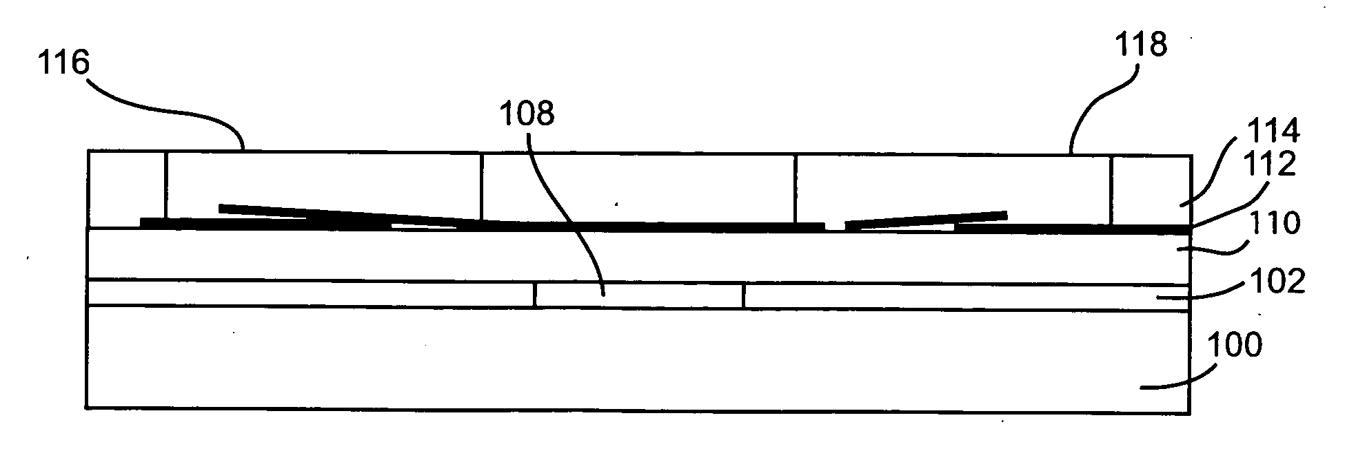
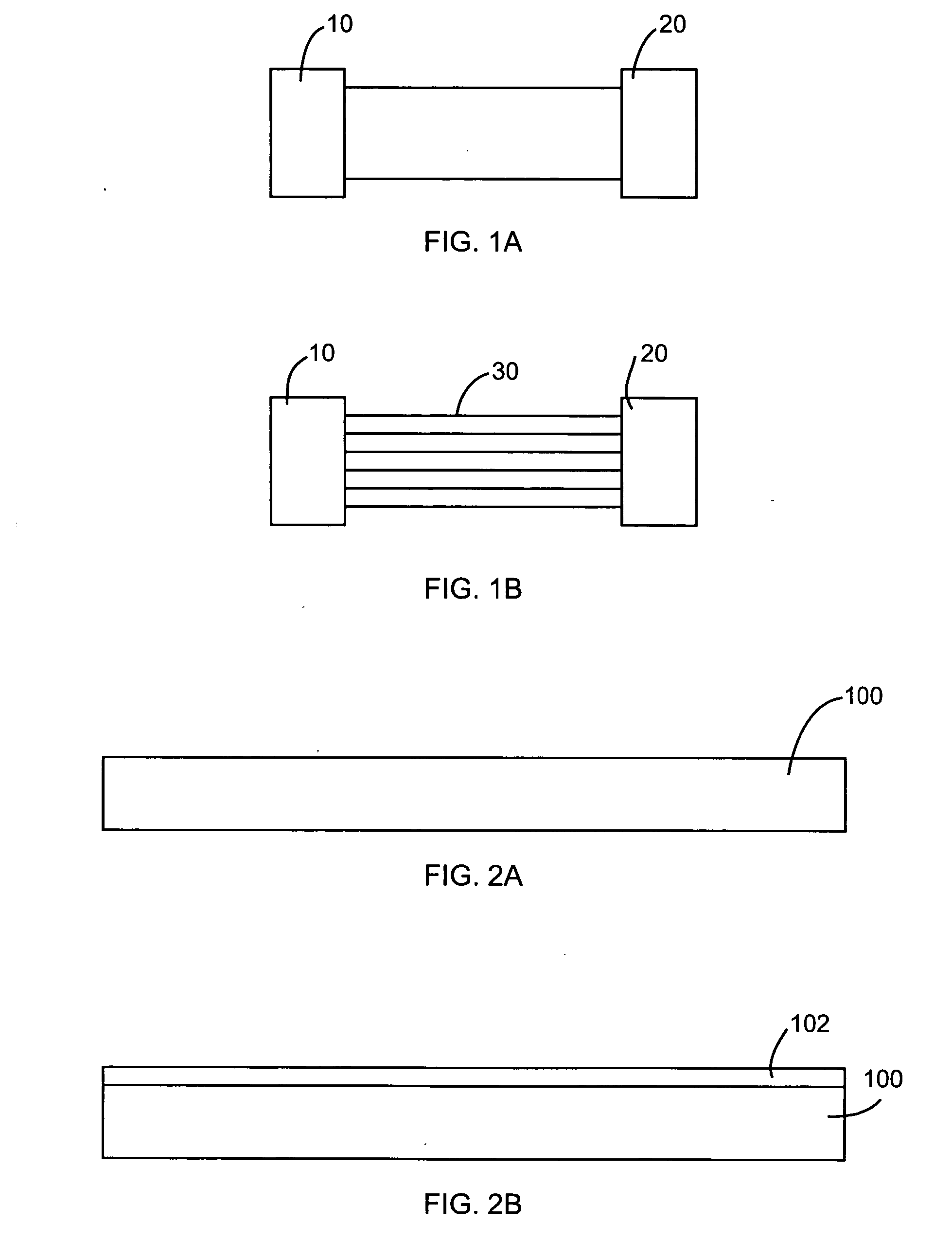
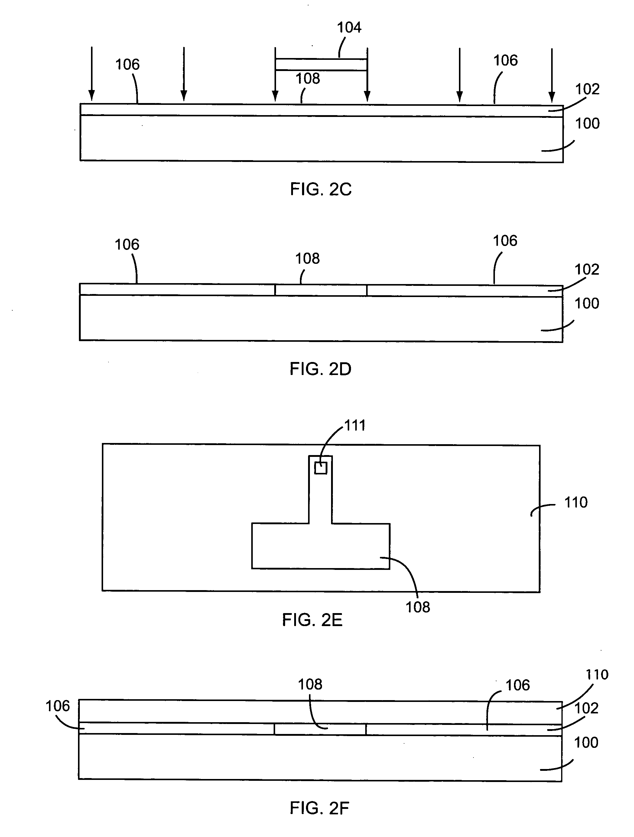
01 Conductive polymer materials for synaptic transistor channels
Conductive polymers serve as the active channel material in synaptic transistors, enabling modulation of conductivity to mimic biological synaptic behavior. These polymers exhibit tunable electrical properties through doping and structural modifications, allowing for precise control of synaptic weight changes. The polymer-based channels can demonstrate both volatile and non-volatile memory characteristics essential for neuromorphic computing applications.- Conductive polymer materials for synaptic transistor channels: Conductive polymers serve as the active channel material in synaptic transistors, enabling modulation of conductivity to mimic biological synaptic behavior. These organic semiconducting polymers provide tunable electrical properties, ion transport capabilities, and compatibility with flexible substrates. The polymer structure allows for electrochemical doping and dedoping processes that simulate synaptic weight changes essential for neuromorphic computing applications.
- Electrolyte-gated organic synaptic transistors: Electrolyte gating mechanisms enable efficient modulation of conductive polymer channels at low operating voltages. The ionic movement within the electrolyte layer controls the doping state of the polymer channel, creating synaptic plasticity effects. This configuration allows for energy-efficient operation and enhanced ionic-electronic coupling, making it suitable for brain-inspired computing devices with low power consumption requirements.
- Polymer composition and doping strategies: The selection and modification of conductive polymer compositions significantly impact synaptic transistor performance. Various doping methods and polymer blends are employed to optimize charge carrier mobility, stability, and switching characteristics. Structural modifications to the polymer backbone and side chains enable fine-tuning of electrical properties, ion permeability, and device retention characteristics for improved synaptic functionality.
- Multilayer device architectures for synaptic functions: Multilayer structures incorporating conductive polymers with dielectric and electrode layers enhance synaptic transistor performance. These architectures enable better control over charge injection, ion migration, and interface properties. The layered design facilitates the implementation of complex synaptic behaviors including short-term and long-term plasticity, paired-pulse facilitation, and spike-timing-dependent plasticity essential for neuromorphic applications.
- Fabrication methods and substrate compatibility: Manufacturing techniques for conductive polymer-based synaptic transistors emphasize solution processing, printing methods, and compatibility with various substrates including flexible and transparent materials. These fabrication approaches enable scalable production, integration with conventional electronics, and development of wearable or implantable neuromorphic devices. Process optimization focuses on achieving uniform polymer films, reliable interfaces, and reproducible device characteristics across large areas.
02 Electrolyte-gated organic synaptic transistors
Electrolyte gating mechanisms combined with conductive polymers enable efficient ion migration and accumulation at polymer interfaces, creating synaptic functionality. This configuration allows for low-voltage operation and high energy efficiency in synaptic devices. The electrolyte layer facilitates electrochemical doping of the conductive polymer channel, resulting in controllable and reversible conductance modulation that emulates synaptic plasticity.Expand Specific Solutions03 Polymer composition and doping strategies for synaptic behavior
Specific polymer compositions and controlled doping methods are critical for achieving desired synaptic characteristics. The selection of conjugated polymer backbones, side chain engineering, and incorporation of dopants influence charge transport properties and switching dynamics. Optimization of polymer molecular weight, crystallinity, and film morphology directly impacts the synaptic weight update linearity and retention time in transistor devices.Expand Specific Solutions04 Multi-terminal synaptic transistor architectures
Advanced device architectures incorporating multiple terminals enable complex synaptic functions beyond simple two-terminal devices. These structures allow independent control of pre-synaptic and post-synaptic signals, facilitating implementation of spike-timing-dependent plasticity and other learning rules. Conductive polymers in multi-terminal configurations provide spatial and temporal integration capabilities essential for neural network hardware implementation.Expand Specific Solutions05 Stability and reliability of polymer-based synaptic devices
Long-term stability and operational reliability of conductive polymer synaptic transistors are enhanced through material encapsulation, interface engineering, and environmental protection strategies. Addressing degradation mechanisms such as oxidation, moisture sensitivity, and electrochemical side reactions is crucial for practical applications. Device lifetime and cycling endurance are improved through polymer formulation optimization and protective layer integration.Expand Specific Solutions
Key Players in Synaptic Computing and Polymer Industries
The synaptic transistors versus conductive polymers technology landscape represents an emerging neuromorphic computing sector in early development stages, with significant growth potential driven by artificial intelligence and edge computing demands. The market remains nascent but shows promising expansion as organizations seek brain-inspired computing solutions for energy-efficient processing. Technology maturity varies considerably across players, with leading research institutions like MIT, Caltech, and Shanghai University advancing fundamental synaptic device physics, while companies such as FUJIFILM Corp., BASF Corp., and DuPont focus on materials development for conductive polymers. Asian institutions including Shenzhen University and Wuhan Textile University contribute specialized materials research, particularly in polymer processing and functionalization. Commercial entities like Nanosys demonstrate quantum dot applications that complement neuromorphic technologies, while chemical manufacturers including Shoei Chemical and Idemitsu Kosan provide essential materials infrastructure. The competitive landscape indicates strong academic-industry collaboration, with technology transfer from universities to commercial applications still developing, suggesting the field requires continued research investment before widespread market adoption.
Massachusetts Institute of Technology
Technical Solution: MIT has developed advanced synaptic transistor architectures using ion-gel gated organic electrochemical transistors (OECTs) that demonstrate synaptic plasticity with conductance modulation ratios exceeding 10^4. Their approach combines organic semiconducting polymers with ionic conductors to create devices that can emulate both short-term and long-term synaptic plasticity. The research focuses on optimizing the polymer-electrolyte interface to achieve low operating voltages (<1V) and high switching speeds. MIT's synaptic transistors show superior temporal dynamics compared to traditional conductive polymer approaches, with the ability to process temporal information through intrinsic device physics rather than external circuitry.
Strengths: Excellent temporal processing capabilities, low power operation, high conductance modulation. Weaknesses: Complex fabrication processes, limited scalability for large arrays.
BASF Corp.
Technical Solution: BASF has developed specialized conductive polymer formulations optimized for neuromorphic computing applications, focusing on improving the stability and performance of organic synaptic devices. Their proprietary polymer blends incorporate novel dopants and stabilizers that enhance the electrochemical switching characteristics while maintaining long-term stability. BASF's materials demonstrate controlled conductance modulation with switching ratios up to 10^3 and operating voltages around 1-2V. The company's approach emphasizes manufacturability and scalability, developing solution-processable materials compatible with roll-to-roll manufacturing. Their conductive polymers show improved environmental stability compared to traditional formulations, with enhanced resistance to oxygen and moisture degradation.
Strengths: Industrial scalability, improved stability, solution-processable manufacturing. Weaknesses: Lower switching ratios compared to transistor approaches, limited speed performance.
Core Innovations in Synaptic Device Materials
MOIRÉ synaptic transistors and applications of same
PatentWO2025111298A9
Innovation
- A moiré synaptic transistor with a top gate, bottom gate, and an asymmetric moiré heterostructure comprising vertically stacked 2D materials like bilayer graphene and hexagonal boron nitride, which enables charge localization and mobile charge distribution, allowing for hysteretic, non-volatile carrier transfers through electron or hole ratcheting, and differential gate control for tunable synaptic plasticity.


Fully integrated organic layered processes for making plastic electronics based on conductive polymers and semiconductor nanowires
PatentInactiveUS20060214156A1
Innovation
- The development of thin film transistors using nanowires or nanoribbons integrated into conductive polymer films, allowing for high carrier mobility and low-temperature fabrication processes, enabling roll-to-roll processing and integration with plastic substrates, which can be patterned using light energy for cost-effective and flexible electronics.

Performance Comparison Framework for Device Selection
Establishing a comprehensive performance comparison framework for synaptic transistors versus conductive polymers requires systematic evaluation across multiple critical dimensions. The framework must address both quantitative metrics and qualitative characteristics that directly impact device selection for neuromorphic computing applications.
The primary performance metrics include switching speed, energy consumption per operation, retention time, and endurance cycles. Synaptic transistors typically demonstrate superior switching speeds in the nanosecond range, while conductive polymer devices often operate in microsecond timeframes. Energy efficiency comparisons reveal that synaptic transistors generally consume femtojoules per synaptic event, whereas conductive polymers may require picojoule-level energy inputs.
Scalability assessment forms another crucial evaluation criterion. This encompasses manufacturing complexity, integration density potential, and cost-effectiveness at volume production. Synaptic transistors benefit from established semiconductor fabrication processes, enabling high-density integration but potentially higher initial costs. Conductive polymers offer advantages in flexible substrates and low-temperature processing but face challenges in achieving consistent device-to-device uniformity.
Reliability metrics must evaluate operational stability under varying environmental conditions, including temperature fluctuations, humidity exposure, and electrical stress. Long-term degradation patterns, failure modes, and predictive lifetime modeling provide essential data for application-specific selection criteria.
The framework should incorporate application-specific weighting factors that reflect the relative importance of different performance parameters. For instance, edge computing applications may prioritize energy efficiency over absolute speed, while high-performance neuromorphic processors might emphasize switching speed and integration density.
Standardized testing protocols ensure consistent evaluation methodology across different device architectures. These protocols must account for measurement variations, statistical significance requirements, and comparative benchmarking against conventional silicon-based solutions to establish meaningful performance baselines for informed device selection decisions.
Integration Challenges in Neuromorphic System Design
The integration of synaptic transistors and conductive polymers into neuromorphic systems presents multifaceted challenges that significantly impact system performance and scalability. These challenges span across material compatibility, fabrication complexity, and system-level optimization requirements.
Material interface compatibility represents a primary integration challenge. Synaptic transistors typically require precise semiconductor processing conditions, including high-temperature annealing and controlled atmospheric environments. Conductive polymers, however, exhibit thermal sensitivity and may degrade under conventional semiconductor processing conditions. This fundamental incompatibility necessitates the development of hybrid fabrication processes that accommodate both material systems without compromising their individual performance characteristics.
Fabrication process integration poses significant technical hurdles. Traditional CMOS fabrication flows must be modified to incorporate organic conductive polymer layers while maintaining the precision required for synaptic transistor arrays. The sequential deposition and patterning of these disparate materials often results in process-induced defects, interface contamination, and yield reduction. Cross-contamination between organic and inorganic processing steps further complicates manufacturing scalability.
Electrical interface design presents another critical challenge. Synaptic transistors and conductive polymers operate under different voltage ranges and current densities. Synaptic transistors typically function at lower voltages with precise current control, while conductive polymers may require higher switching voltages and exhibit different impedance characteristics. Designing interface circuits that effectively bridge these electrical domains while maintaining signal integrity requires sophisticated analog circuit design approaches.
Thermal management becomes increasingly complex in hybrid systems. Conductive polymers generate heat during switching operations and exhibit temperature-dependent conductivity variations. Synaptic transistors require stable operating temperatures for consistent synaptic weight updates. The thermal coupling between these components can lead to performance drift and reliability issues, necessitating advanced thermal design strategies and potentially active cooling solutions.
System-level routing and interconnect design face unique constraints. The different geometries and connection requirements of synaptic transistor arrays versus conductive polymer networks create routing congestion and signal delay mismatches. Optimizing the physical layout to minimize parasitic effects while ensuring adequate connectivity between heterogeneous components requires novel design automation tools and methodologies.
Reliability and aging characteristics differ significantly between the two technologies. Synaptic transistors may exhibit gradual parameter drift over extended operation periods, while conductive polymers can experience more abrupt failure modes related to polymer chain degradation. Developing unified reliability models and compensation strategies for hybrid systems remains an ongoing challenge that impacts long-term system viability and commercial deployment prospects.
Unlock deeper insights with PatSnap Eureka Quick Research — get a full tech report to explore trends and direct your research. Try now!
Generate Your Research Report Instantly with AI Agent
Supercharge your innovation with PatSnap Eureka AI Agent Platform!