

How to Leverage Synaptic Transistors in Edge Computing
APR 17, 20269 MIN READ
Generate Your Research Report Instantly with AI Agent
Patsnap Eureka helps you evaluate technical feasibility & market potential.
Synaptic Transistor Edge Computing Background and Objectives
The convergence of neuromorphic computing and edge computing represents a paradigm shift in how we approach distributed intelligence systems. Synaptic transistors, inspired by biological neural synapses, have emerged as a revolutionary technology that mimics the adaptive learning mechanisms found in the human brain. These devices can simultaneously process and store information, fundamentally departing from the traditional von Neumann architecture that separates computation and memory functions.
Edge computing has gained tremendous momentum as organizations seek to reduce latency, enhance privacy, and minimize bandwidth requirements by processing data closer to its source. However, conventional edge devices face significant limitations in power consumption, computational efficiency, and real-time learning capabilities. The integration of synaptic transistors into edge computing architectures presents an unprecedented opportunity to address these challenges while enabling intelligent, adaptive systems at the network periphery.
The historical development of synaptic transistors traces back to early neuromorphic research in the 1980s, with significant breakthroughs occurring in the past decade through advances in materials science and nanotechnology. Key milestones include the development of memristive devices, organic synaptic transistors, and ion-gated transistors that exhibit plasticity characteristics similar to biological synapses. These devices demonstrate the ability to modulate conductance based on input history, enabling in-situ learning and adaptation.
The primary objective of leveraging synaptic transistors in edge computing is to create ultra-low-power, intelligent edge devices capable of real-time learning and decision-making without relying on cloud connectivity. This technology aims to enable distributed artificial intelligence systems that can adapt to local conditions, learn from environmental changes, and make autonomous decisions with minimal energy consumption.
Secondary objectives include developing scalable neuromorphic architectures that can handle complex pattern recognition tasks, implementing fault-tolerant systems that maintain functionality despite device variations, and creating standardized interfaces that allow seamless integration with existing edge computing infrastructure. The ultimate goal is to establish a new computing paradigm that combines the efficiency of biological neural networks with the reliability and scalability of modern semiconductor technology.
Market Demand for Neuromorphic Edge Computing Solutions
The global edge computing market is experiencing unprecedented growth driven by the proliferation of Internet of Things devices, autonomous systems, and real-time applications requiring ultra-low latency processing. Traditional von Neumann architectures face significant limitations in power efficiency and computational speed when deployed at the edge, creating substantial demand for alternative computing paradigms. Neuromorphic edge computing solutions leveraging synaptic transistors represent a transformative approach to address these critical market needs.
Industrial automation and smart manufacturing sectors demonstrate particularly strong demand for neuromorphic edge solutions. Manufacturing facilities require real-time sensor data processing, predictive maintenance capabilities, and adaptive control systems that can operate efficiently in harsh environments with minimal power consumption. Synaptic transistor-based systems offer the ability to perform complex pattern recognition and decision-making tasks locally, reducing dependency on cloud connectivity and enabling autonomous operation during network disruptions.
The autonomous vehicle industry presents another significant market opportunity for neuromorphic edge computing. Advanced driver assistance systems and fully autonomous vehicles generate massive amounts of sensor data requiring immediate processing for safety-critical decisions. Traditional edge computing solutions struggle with the power and thermal constraints of automotive environments while maintaining the computational performance necessary for real-time object detection, path planning, and collision avoidance. Neuromorphic architectures using synaptic transistors can dramatically reduce power consumption while providing the parallel processing capabilities essential for automotive applications.
Healthcare and medical device markets are increasingly demanding intelligent edge computing solutions for wearable devices, implantable sensors, and portable diagnostic equipment. These applications require continuous monitoring and analysis of physiological signals while operating under strict power budgets. Synaptic transistor-based neuromorphic processors can enable sophisticated signal processing and anomaly detection capabilities in battery-powered medical devices, extending operational lifetime and improving patient outcomes through continuous health monitoring.
Smart city infrastructure represents an emerging market segment with substantial growth potential for neuromorphic edge computing solutions. Traffic management systems, environmental monitoring networks, and public safety applications require distributed intelligence capable of processing multiple data streams simultaneously while maintaining low power consumption. The ability of synaptic transistors to perform in-memory computing and adapt to changing environmental conditions makes them particularly suitable for these dynamic urban applications.
The convergence of artificial intelligence workloads with edge computing requirements is driving demand for specialized hardware architectures that can efficiently execute neural network inference tasks. Synaptic transistors offer inherent advantages for implementing spiking neural networks and other bio-inspired computing models that align naturally with edge computing constraints and real-world sensor data characteristics.
Current State and Challenges of Synaptic Transistor Technology
Synaptic transistors represent a paradigm shift in neuromorphic computing, mimicking the behavior of biological synapses through their ability to modulate conductance states based on input history. These devices integrate memory and processing functions within a single component, offering significant advantages over traditional von Neumann architectures. Current implementations primarily utilize organic electrochemical transistors, ferroelectric field-effect transistors, and memristive devices that can exhibit synaptic plasticity through various physical mechanisms including ion migration, charge trapping, and phase transitions.
The global development of synaptic transistor technology shows significant geographical concentration, with leading research institutions predominantly located in the United States, South Korea, China, and European Union countries. Major technological hubs include Stanford University, MIT, Samsung Advanced Institute of Technology, Tsinghua University, and IMEC in Belgium. These institutions have collectively advanced the field through breakthrough demonstrations in device fabrication, material engineering, and circuit integration methodologies.
Despite substantial progress, several critical challenges impede the widespread adoption of synaptic transistors in edge computing applications. Device variability remains a primary concern, as manufacturing inconsistencies lead to unpredictable synaptic weights and learning behaviors that compromise neural network accuracy. Current fabrication processes struggle to achieve the precision required for large-scale integration, with device-to-device variations often exceeding acceptable tolerances for reliable computation.
Endurance and retention characteristics present additional obstacles for practical deployment. Many synaptic transistor implementations suffer from limited write-erase cycles and gradual conductance drift over time, which degrades the stored synaptic weights and necessitates frequent recalibration. The temporal stability of synaptic states varies significantly across different material systems, with organic devices typically showing shorter retention times compared to inorganic alternatives.
Power consumption optimization remains an ongoing challenge, particularly for battery-powered edge devices. While synaptic transistors theoretically offer energy-efficient computation through event-driven processing, current implementations often require higher operating voltages than desired for ultra-low-power applications. The trade-off between switching speed, power consumption, and retention time continues to constrain device optimization efforts.
Integration complexity poses significant hurdles for system-level implementation. Current synaptic transistor technologies require specialized peripheral circuits for programming, reading, and maintaining synaptic states. The lack of standardized fabrication processes compatible with existing CMOS technology limits scalability and increases manufacturing costs, hindering commercial viability for edge computing applications.
Current Synaptic Transistor Implementation Approaches
01 Organic semiconductor-based synaptic transistors
Synaptic transistors can be fabricated using organic semiconductor materials to mimic biological synaptic functions. These devices utilize organic thin-film transistor structures with ion-gel or electrolyte gates to achieve synaptic plasticity, including short-term and long-term potentiation and depression. The organic materials provide advantages such as flexibility, low-cost fabrication, and biocompatibility, making them suitable for neuromorphic computing applications.- Organic semiconductor materials for synaptic transistors: Synaptic transistors can be fabricated using organic semiconductor materials that exhibit neuromorphic behavior. These materials enable the device to mimic biological synapses by modulating conductance states in response to electrical stimuli. Organic materials offer advantages such as flexibility, low-cost processing, and compatibility with large-area electronics. The use of organic semiconductors in synaptic transistors allows for the development of artificial neural networks and neuromorphic computing systems.
- Ion-gated transistor structures for synaptic functionality: Ion-gated transistor configurations utilize ionic species to modulate channel conductance, mimicking the ion-based signaling in biological synapses. These structures typically employ electrolyte materials or ion-conducting layers that enable dynamic control of synaptic weight through ion migration. The ion-gating mechanism provides analog memory characteristics and low-power operation suitable for neuromorphic applications. This approach enables the implementation of synaptic plasticity including short-term and long-term potentiation.
- Multi-terminal synaptic transistor architectures: Multi-terminal transistor designs incorporate additional gate electrodes or terminals to enhance synaptic functionality and enable complex neural operations. These architectures allow independent control of multiple synaptic parameters and facilitate the implementation of advanced learning rules. The multi-terminal configuration enables simultaneous excitatory and inhibitory functions within a single device. Such structures provide improved integration density and functional versatility for neuromorphic circuits.
- Two-dimensional materials for synaptic devices: Two-dimensional materials such as transition metal dichalcogenides and graphene derivatives are employed as channel materials in synaptic transistors. These materials exhibit unique electronic properties including high carrier mobility, atomic-scale thickness, and tunable bandgaps that are beneficial for synaptic operations. The atomically thin nature of these materials enables efficient electrostatic control and low-power switching. Integration of two-dimensional materials facilitates the fabrication of high-performance synaptic devices with excellent scalability.
- Ferroelectric and memristive mechanisms in synaptic transistors: Ferroelectric materials and memristive elements are integrated into transistor structures to achieve non-volatile synaptic weight storage and analog conductance modulation. These mechanisms rely on polarization switching or resistance changes that can be programmed by electrical pulses to emulate synaptic plasticity. The non-volatile nature of these effects enables energy-efficient operation by eliminating the need for constant power to maintain synaptic states. Such devices demonstrate multiple conductance levels and gradual switching characteristics essential for neuromorphic learning.
02 Two-dimensional material-based synaptic devices
Two-dimensional materials such as graphene, transition metal dichalcogenides, and other layered materials can be employed to construct synaptic transistors with enhanced performance. These materials offer unique electronic properties including high carrier mobility, atomic-scale thickness, and tunable bandgaps. The synaptic devices based on two-dimensional materials demonstrate excellent switching characteristics, low power consumption, and the ability to emulate various synaptic behaviors for artificial neural networks.Expand Specific Solutions03 Ferroelectric and memristive synaptic transistors
Ferroelectric materials and memristive structures can be integrated into transistor architectures to create synaptic devices with non-volatile memory characteristics. These devices leverage polarization switching in ferroelectric materials or resistance changes in memristive elements to store synaptic weights. The combination of transistor control and memory functionality enables efficient implementation of synaptic learning rules and weight updates in neuromorphic systems.Expand Specific Solutions04 Multi-terminal synaptic transistor configurations
Advanced synaptic transistor designs incorporate multiple terminals to enable complex synaptic functions and improved control over device operation. These multi-terminal structures allow for independent modulation of pre-synaptic and post-synaptic signals, implementation of spike-timing-dependent plasticity, and enhanced integration density. The configurations may include dual-gate, tri-gate, or other multi-electrode arrangements to achieve sophisticated neuromorphic functionalities.Expand Specific Solutions05 Synaptic transistor arrays and neuromorphic circuits
Integration of synaptic transistors into array configurations and neuromorphic circuit architectures enables the construction of artificial neural networks for computing applications. These systems incorporate crossbar arrays, interconnection schemes, and peripheral circuitry to implement neural network operations such as pattern recognition, classification, and learning. The array-based approach provides scalability and parallel processing capabilities for efficient neuromorphic computing.Expand Specific Solutions
Key Players in Synaptic Transistor and Edge Computing
The synaptic transistor technology for edge computing represents an emerging field in the early development stage, with significant growth potential driven by increasing demand for neuromorphic computing solutions. The market remains relatively nascent but shows promising expansion as edge AI applications proliferate. Technology maturity varies considerably across key players, with established semiconductor giants like Intel, NVIDIA, and Qualcomm leading commercial development, while companies such as Infineon Technologies, Analog Devices, and ARM contribute specialized components and architectures. Research institutions including Peking University, KAIST, and Gwangju Institute of Science & Technology are advancing fundamental breakthroughs in synaptic device physics and neural network implementations. The competitive landscape features a mix of traditional chip manufacturers adapting existing technologies and innovative startups developing novel neuromorphic approaches, creating a dynamic ecosystem poised for substantial technological advancement.
Huawei Technologies Co., Ltd.
Technical Solution: Huawei has developed neuromorphic computing solutions that integrate synaptic transistors for edge AI applications. Their approach focuses on memristor-based synaptic devices that can perform in-memory computing, reducing data movement between memory and processing units. The company's synaptic transistor technology enables real-time learning and adaptation in edge devices, particularly for mobile and IoT applications. Their implementation supports both supervised and unsupervised learning algorithms directly in hardware, achieving significant power efficiency improvements compared to traditional von Neumann architectures. The technology is designed to handle dynamic workloads while maintaining low latency and energy consumption, making it suitable for battery-powered edge devices.
Strengths: Strong integration capabilities with existing mobile platforms, excellent power efficiency optimization. Weaknesses: Limited availability due to geopolitical restrictions, relatively new technology with unproven long-term reliability.
NVIDIA Corp.
Technical Solution: NVIDIA leverages synaptic transistor concepts in their edge computing platforms through neuromorphic processing units integrated with their Jetson series. Their approach combines traditional GPU architecture with synaptic computing elements to enable efficient neural network inference at the edge. The company's synaptic transistor implementation focuses on spike-based neural networks that can process temporal data streams with minimal power consumption. Their technology supports event-driven computation, where synaptic transistors only activate when receiving input spikes, dramatically reducing power consumption during idle periods. NVIDIA's solution is particularly optimized for computer vision and sensor fusion applications in autonomous systems.
Strengths: Mature ecosystem with comprehensive software support, proven performance in AI workloads. Weaknesses: Higher power consumption compared to pure neuromorphic solutions, premium pricing limits adoption in cost-sensitive applications.
Core Patents in Synaptic Transistor Edge Applications
MOIRÉ synaptic transistors and applications of same
PatentWO2025111298A9
Innovation
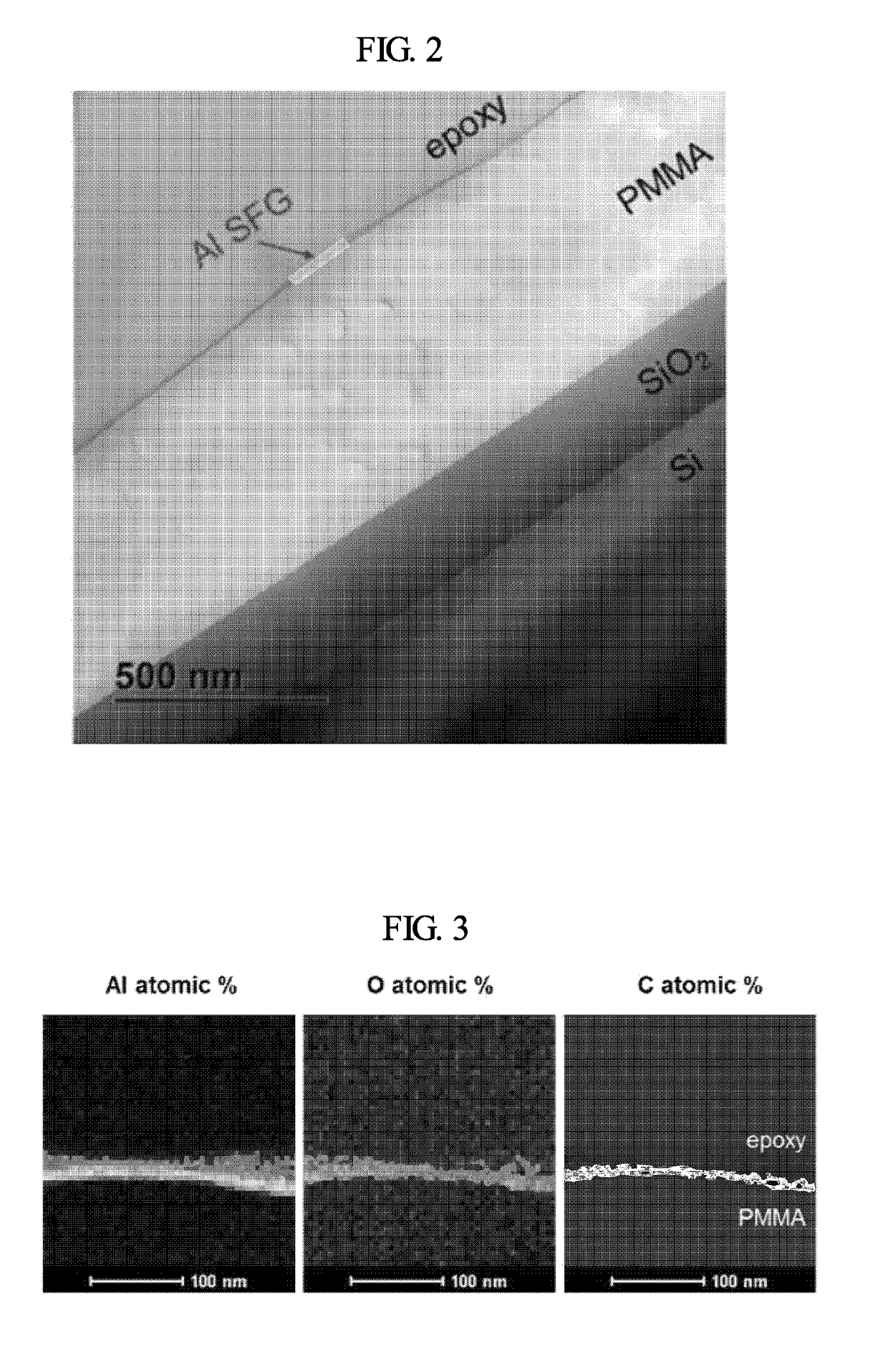
- A moiré synaptic transistor with a top gate, bottom gate, and an asymmetric moiré heterostructure comprising vertically stacked 2D materials like bilayer graphene and hexagonal boron nitride, which enables charge localization and mobile charge distribution, allowing for hysteretic, non-volatile carrier transfers through electron or hole ratcheting, and differential gate control for tunable synaptic plasticity.


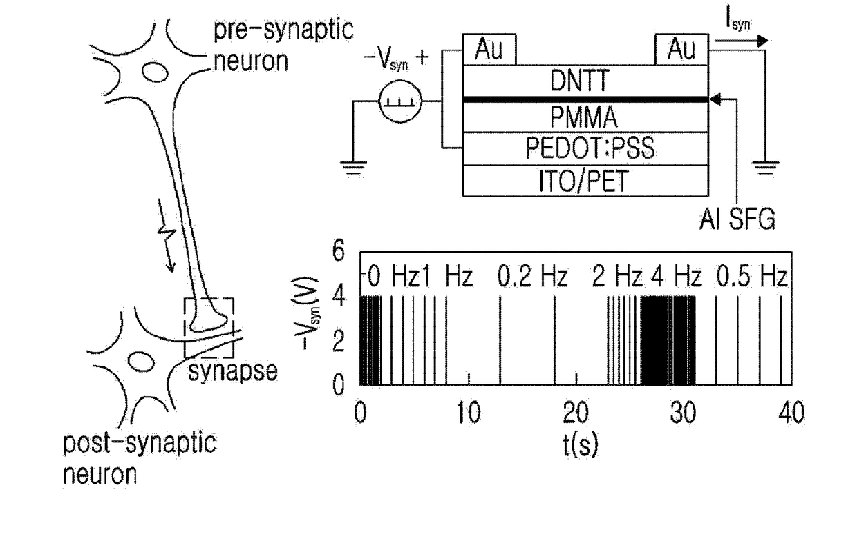
Synaptic transistor based on metal nano-sheet and method of manufacturing the same
PatentActiveUS20180083212A1
Innovation
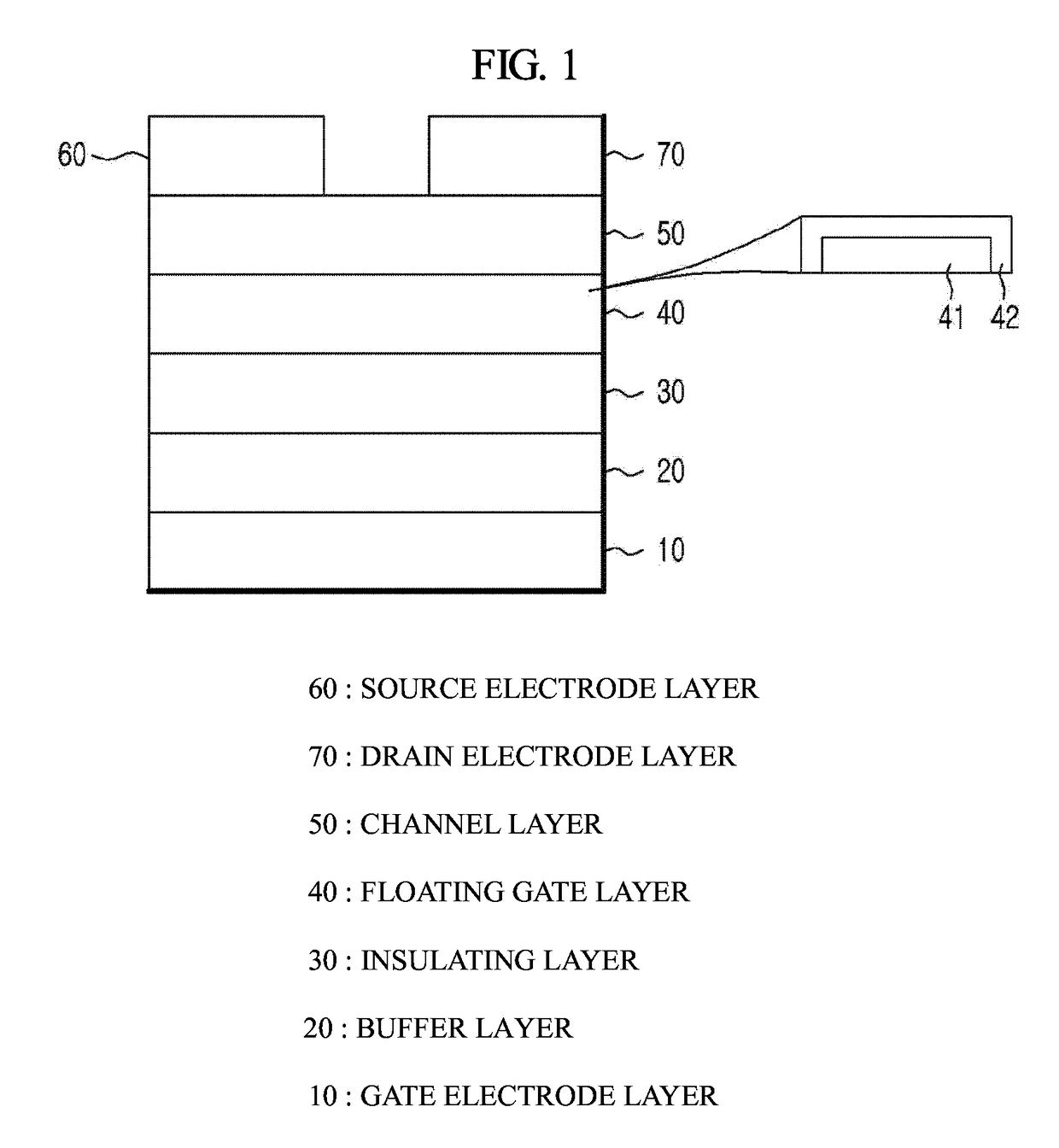
- A synaptic transistor based on a metal nano-sheet structure, featuring a gate electrode layer, buffer layer, insulating layer, self-assembled floating gate layer, source electrode layer, and drain electrode layer, where the self-assembled floating gate layer includes naturally oxidizing materials like silver, copper, or aluminum, and a metal oxide layer for efficient charge storage and isolation.

Energy Efficiency Standards for Edge Computing Devices
The integration of synaptic transistors in edge computing devices necessitates the establishment of comprehensive energy efficiency standards to ensure optimal performance while maintaining sustainable power consumption. Current industry standards primarily focus on traditional silicon-based processors, leaving a significant gap in addressing the unique energy characteristics of neuromorphic computing elements.
Existing energy efficiency frameworks, such as ENERGY STAR and IEEE 1621 standards, provide baseline metrics for conventional computing devices but lack specific provisions for synaptic transistor architectures. These neuromorphic components exhibit fundamentally different power consumption patterns, characterized by event-driven processing and adaptive energy scaling based on computational load. Traditional metrics like performance-per-watt become insufficient when evaluating devices that dynamically adjust their energy consumption based on synaptic activity levels.
The development of specialized energy efficiency standards for synaptic transistor-based edge devices requires new measurement methodologies that account for their unique operational characteristics. Key parameters should include synaptic switching energy, standby power consumption during inactive states, and energy efficiency across varying spike frequencies. These standards must also consider the temporal aspects of neuromorphic processing, where energy consumption fluctuates significantly based on input data patterns and learning phases.
International standardization bodies are beginning to recognize the need for neuromorphic-specific energy metrics. The IEEE Standards Association has initiated preliminary discussions on establishing benchmarks that incorporate synaptic plasticity energy costs and long-term potentiation power requirements. These emerging standards aim to create unified testing protocols that enable fair comparison between different synaptic transistor implementations and traditional computing solutions.
Implementation of these energy efficiency standards will require collaboration between semiconductor manufacturers, edge computing vendors, and regulatory bodies. The standards must balance performance requirements with environmental sustainability goals while ensuring practical applicability across diverse edge computing applications. This standardization effort will ultimately drive innovation in low-power synaptic transistor designs and accelerate their adoption in energy-constrained edge computing environments.
Hardware-Software Co-design for Neuromorphic Edge Systems
The integration of synaptic transistors into edge computing systems necessitates a fundamental shift from traditional hardware-software paradigms toward co-designed neuromorphic architectures. This approach recognizes that synaptic transistors operate fundamentally differently from conventional CMOS devices, requiring specialized software frameworks that can exploit their inherent plasticity and analog computing capabilities.
Hardware-software co-design for neuromorphic edge systems begins with the development of specialized compiler toolchains that can map neural network operations directly onto synaptic transistor arrays. These compilers must understand the unique characteristics of synaptic devices, including their conductance modulation ranges, switching dynamics, and variability patterns. The software stack needs to incorporate device-aware optimization algorithms that can adapt network weights and architectures to match the physical constraints and capabilities of the underlying synaptic hardware.
The operating system layer requires significant modifications to support neuromorphic computing paradigms. Traditional von Neumann architectures separate memory and processing, while synaptic transistors inherently combine these functions. New scheduling algorithms must be developed to manage the temporal dynamics of synaptic plasticity, ensuring that learning and inference operations are properly coordinated across distributed synaptic arrays.
Programming models for neuromorphic edge systems must abstract the complexity of synaptic device physics while providing developers with intuitive interfaces for implementing neural algorithms. Event-driven programming frameworks show particular promise, as they align naturally with the spike-based communication protocols commonly used in neuromorphic systems. These frameworks enable efficient handling of sparse, asynchronous data streams typical in edge computing scenarios.
Cross-layer optimization represents a critical aspect of hardware-software co-design, where application requirements directly influence hardware configuration and vice versa. For instance, power management strategies must consider both the software workload characteristics and the physical properties of synaptic devices, such as their retention times and switching energy requirements. This holistic approach enables the development of adaptive systems that can dynamically reconfigure both hardware parameters and software execution patterns based on real-time performance metrics and environmental conditions.
Unlock deeper insights with Patsnap Eureka Quick Research — get a full tech report to explore trends and direct your research. Try now!
Generate Your Research Report Instantly with AI Agent
Supercharge your innovation with Patsnap Eureka AI Agent Platform!