

Heterogeneous Integration Hybrid Bonding: Alignment, Void Control And Reliability
SEP 19, 20259 MIN READ
Generate Your Research Report Instantly with AI Agent
PatSnap Eureka helps you evaluate technical feasibility & market potential.
Hybrid Bonding Technology Evolution and Objectives
Hybrid bonding technology represents a significant advancement in semiconductor packaging, evolving from traditional wire bonding and flip-chip technologies to enable higher density interconnects with improved electrical and thermal performance. The journey of hybrid bonding began in the early 2000s with initial research into direct copper-to-copper bonding techniques, primarily focused on image sensor applications. By 2010, the technology had expanded to include dielectric-to-dielectric bonding, creating a more robust interconnection system.
The fundamental principle of hybrid bonding involves the simultaneous bonding of metal and dielectric materials between two wafers or dies, typically achieved through a combination of thermal compression and chemical reactions. This approach eliminates the need for intermediate materials like solder bumps or underfill, resulting in finer pitch capabilities and reduced parasitic effects.
A critical milestone in hybrid bonding evolution occurred around 2016 when major semiconductor manufacturers began implementing hybrid bonding in high-volume production, particularly for advanced memory-logic integration. This transition from research to commercial application demonstrated the technology's viability for addressing the increasing demands of heterogeneous integration in advanced computing architectures.
The primary objectives of current hybrid bonding technology development center on three key challenges: alignment precision, void control, and long-term reliability. As interconnect pitches continue to shrink below 10μm, alignment accuracy requirements have become increasingly stringent, necessitating innovations in both equipment and processes. Simultaneously, the formation of voids at bonding interfaces remains a persistent challenge that impacts both yield and reliability.
Looking forward, the technology roadmap for hybrid bonding aims to achieve sub-micron pitch interconnects while maintaining high throughput and yield. This will require significant advancements in surface preparation techniques, alignment systems, and bonding process control. Additionally, there is growing interest in extending hybrid bonding capabilities to accommodate greater diversity in material combinations and to support room-temperature or near-room-temperature bonding processes.
The ultimate goal of hybrid bonding technology evolution is to enable true heterogeneous integration, where disparate components manufactured using different process technologies can be seamlessly combined with minimal electrical, thermal, or mechanical penalties. This capability is increasingly critical for next-generation computing architectures, including artificial intelligence accelerators, high-performance computing systems, and advanced mobile devices.
Market Demand Analysis for Advanced Packaging Solutions
The advanced packaging market is experiencing unprecedented growth, driven by the increasing demand for smaller, faster, and more power-efficient electronic devices. Heterogeneous Integration (HI) through hybrid bonding has emerged as a critical technology to meet these demands, with the global advanced packaging market projected to reach $42 billion by 2025, growing at a CAGR of 10.2% from 2020.
Consumer electronics remains the largest application segment, accounting for approximately 35% of the market share. The proliferation of smartphones, wearables, and IoT devices has created substantial demand for compact, high-performance packaging solutions that can integrate diverse functionalities while maintaining reliability. Hybrid bonding technology addresses these needs by enabling direct copper-to-copper connections without intermediate materials, resulting in finer pitches and higher interconnect densities.
The automotive sector represents the fastest-growing market segment for advanced packaging, with an estimated growth rate of 15% annually. As vehicles incorporate more advanced driver-assistance systems (ADAS) and move toward autonomous driving capabilities, the need for reliable, high-performance computing modules that can withstand harsh environmental conditions has intensified. Hybrid bonding offers superior thermal performance and mechanical stability compared to traditional packaging methods, making it particularly suitable for automotive applications.
Data centers and high-performance computing applications are driving demand for packaging solutions that can manage increasing data volumes and computational requirements while minimizing power consumption. The need for efficient heat dissipation and higher bandwidth has positioned hybrid bonding as a preferred solution, with its ability to reduce interconnect lengths and improve thermal management.
Geographically, Asia-Pacific dominates the advanced packaging market with approximately 65% share, led by Taiwan, South Korea, and China. North America follows with 20% market share, primarily driven by demand from data centers and defense applications. Europe accounts for 12% of the market, with significant growth in automotive electronics applications.
The COVID-19 pandemic initially disrupted supply chains but subsequently accelerated digitalization trends, creating stronger long-term demand for advanced packaging solutions. Industry analysts predict that hybrid bonding will capture an increasing share of the advanced packaging market, growing from less than 5% currently to potentially 15-20% by 2027, as alignment precision improves and void control techniques mature.
Key customer requirements driving market adoption include improved thermal performance, higher interconnect density, enhanced reliability, and cost-effectiveness. Manufacturers who can address the technical challenges of alignment precision, void control, and reliability testing stand to capture significant market share in this rapidly evolving landscape.
Current Challenges in Heterogeneous Integration Bonding
Heterogeneous integration hybrid bonding faces several critical challenges that impede its widespread adoption in advanced semiconductor packaging. The alignment precision requirements have become increasingly stringent, with current technologies demanding sub-micron accuracy (typically <0.5μm) to ensure proper electrical connections between bonding pads. This precision becomes exponentially more difficult to achieve as die sizes increase and pad pitches decrease below 10μm, creating significant manufacturing complexity.
Void formation during the bonding process represents another major obstacle. These microscopic cavities can form due to surface contamination, trapped gases, or inadequate surface preparation. Even nanometer-scale voids can compromise electrical connectivity, thermal performance, and long-term reliability. Current detection methods struggle to identify sub-surface voids non-destructively, making quality control particularly challenging.
Surface preparation quality significantly impacts bonding success. The surfaces must achieve specific roughness parameters (typically <1nm RMS) and be free from organic residues, particles, and oxide layers. Maintaining this cleanliness in production environments presents considerable difficulties, especially when scaling to high-volume manufacturing where even minor contamination can cause catastrophic bond failures.
Thermal management during and after bonding poses additional challenges. The coefficient of thermal expansion (CTE) mismatch between different materials can generate significant stress at bonding interfaces during temperature cycling. This stress may lead to delamination, cracking, or complete bond failure over time. The industry lacks standardized reliability testing protocols specifically designed for hybrid bonded structures, making long-term performance prediction difficult.
Process integration complexity further complicates matters. Hybrid bonding must be compatible with existing semiconductor fabrication processes, including wafer thinning, through-silicon via (TSV) formation, and redistribution layer (RDL) processing. Each integration step introduces potential failure modes and yield impacts that must be carefully managed.
Equipment limitations also present barriers to advancement. Current bonding tools struggle to simultaneously achieve the required alignment precision, temperature uniformity, and pressure control across large wafers. Additionally, inspection equipment capable of non-destructively evaluating bond quality at high throughput remains underdeveloped, creating bottlenecks in production environments.
Cost considerations remain significant, as specialized equipment, clean room requirements, and yield challenges contribute to higher manufacturing expenses compared to traditional packaging methods. This cost premium must be justified by performance improvements to drive broader industry adoption.
Existing Alignment and Void Control Methodologies
01 Alignment techniques for hybrid bonding in heterogeneous integration
Precise alignment is critical for successful hybrid bonding in heterogeneous integration. Advanced alignment techniques include optical alignment systems, infrared alignment through silicon, and mechanical alignment features. These methods ensure accurate positioning of different semiconductor materials or components before bonding, minimizing misalignment issues that could lead to connection failures or reduced performance in the integrated devices.- Alignment techniques for hybrid bonding in heterogeneous integration: Precise alignment is critical for successful hybrid bonding in heterogeneous integration. Advanced alignment techniques include optical alignment systems, infrared alignment through silicon, and mechanical alignment features. These methods ensure accurate positioning of different semiconductor components before bonding, minimizing misalignment issues that could lead to electrical connection failures or structural weaknesses. High-precision alignment tools can achieve sub-micron accuracy, which is essential for modern high-density interconnects.
- Void control strategies in hybrid bonding processes: Controlling voids during hybrid bonding is essential for ensuring reliable connections. Techniques include surface preparation methods such as chemical-mechanical polishing, plasma activation, and specialized cleaning processes to remove contaminants and ensure smooth bonding surfaces. Controlled bonding environments with specific temperature, pressure, and atmospheric conditions help minimize void formation. Post-bonding annealing processes can also reduce voids by promoting material flow and enhancing bond strength.
- Reliability enhancement methods for heterogeneous integration: Improving the reliability of heterogeneously integrated devices involves multiple approaches. These include stress management techniques to address coefficient of thermal expansion mismatches, barrier layers to prevent diffusion and contamination, and specialized bonding materials that can withstand thermal cycling. Testing methodologies such as accelerated aging tests, thermal shock testing, and mechanical stress testing help validate long-term reliability. Design considerations like redundant connections and optimized layout patterns further enhance overall system reliability.
- Advanced inspection and quality control for hybrid bonding: Inspection and quality control are crucial for successful hybrid bonding. Non-destructive testing methods include acoustic microscopy, X-ray imaging, and infrared thermography to detect voids, cracks, and delamination. In-line monitoring systems track critical parameters during the bonding process, allowing for real-time adjustments. Advanced imaging techniques with high resolution capabilities can detect sub-micron defects. Statistical process control methods help maintain consistent quality across high-volume manufacturing.
- Material innovations for hybrid bonding interfaces: Novel materials are being developed to improve hybrid bonding performance. These include specialized dielectric materials with optimized mechanical and electrical properties, metal systems designed for low-temperature bonding, and composite bonding layers that can accommodate stress. Surface functionalization techniques modify interface chemistry to enhance adhesion. Self-healing materials that can repair minor defects during thermal processing are also being explored to improve long-term reliability and reduce void formation.
02 Void control strategies in hybrid bonding processes
Controlling voids during hybrid bonding is essential for ensuring reliable connections. Techniques include surface preparation methods such as chemical mechanical polishing, plasma activation, and specialized cleaning processes to remove contaminants. Additionally, controlled bonding environments with specific temperature, pressure, and atmospheric conditions help minimize void formation. Some approaches incorporate intermediate layers or specific bonding sequences to reduce trapped gases and improve interface quality.Expand Specific Solutions03 Reliability enhancement methods for heterogeneous integration
Improving the reliability of heterogeneously integrated devices involves multiple approaches including thermal management techniques, stress mitigation designs, and specialized testing protocols. Thermal cycling tests, humidity tests, and mechanical stress tests are employed to evaluate bond integrity. Advanced materials with matched coefficient of thermal expansion help reduce stress at interfaces. Some methods incorporate redundant connection designs or self-healing materials to improve long-term reliability under various operating conditions.Expand Specific Solutions04 Inspection and quality control for hybrid bonding
Non-destructive inspection techniques are crucial for quality control in hybrid bonding processes. These include acoustic microscopy, X-ray imaging, infrared thermography, and electrical testing methods to detect voids, misalignments, or weak bonds. In-line monitoring systems provide real-time feedback during the bonding process, allowing for immediate adjustments. Advanced image processing algorithms help analyze bonding interfaces and predict potential reliability issues before device completion.Expand Specific Solutions05 Novel materials and surface treatments for improved hybrid bonding
Innovative materials and surface treatments significantly enhance hybrid bonding performance. These include specialized dielectric materials with optimized bonding properties, metal systems designed for low-temperature bonding, and surface functionalization techniques that improve adhesion. Plasma treatments, chemical activations, and nanoscale surface modifications create more reactive surfaces for stronger bonds. Some approaches incorporate intermediate bonding layers or nanostructured surfaces that facilitate better connections between dissimilar materials.Expand Specific Solutions
Leading Companies in Hybrid Bonding Ecosystem
Heterogeneous Integration Hybrid Bonding technology is currently in the early growth phase, characterized by rapid innovation and expanding applications in advanced semiconductor packaging. The market is projected to grow significantly as demand for higher performance and miniaturization increases in computing, AI, and mobile applications. Leading semiconductor manufacturers like TSMC, Intel, and Samsung are investing heavily in this technology, while equipment providers such as Applied Materials, Tokyo Electron, and EV Group are developing specialized tools for alignment precision and void control. Research institutions including IBM and Shanghai Integrated Circuit Research & Development Center are addressing key technical challenges in reliability and yield improvement. The technology is approaching commercial maturity with several companies transitioning from R&D to production implementation.
Intel Corp.
Technical Solution: Intel has developed Embedded Multi-die Interconnect Bridge (EMIB) and Foveros 3D packaging technologies that incorporate hybrid bonding elements. Their approach focuses on precise die-to-die alignment using fiducial marks and machine vision systems capable of sub-micron alignment accuracy. For void control, Intel employs a combination of surface activation techniques and controlled atmosphere bonding environments to minimize trapped gases. Their Direct Hybrid Bonding (DHB) technology utilizes specialized surface preparation with multi-stage cleaning and planarization to achieve surface roughness below 0.3nm[3]. Intel's reliability enhancement strategy includes stress-relieving buffer layers and optimized thermal profiles during the bonding process. They've implemented in-line metrology systems for real-time monitoring of bond quality and developed accelerated testing protocols that simulate up to 10 years of operational conditions to verify long-term reliability[4]. Their recent advancements include development of self-aligning bonding structures that can compensate for minor misalignments during the thermal compression process.
Strengths: Advanced in-line metrology capabilities, comprehensive reliability testing infrastructure, and integration with their established manufacturing processes. Their self-aligning structures improve yield rates. Weaknesses: Their hybrid bonding technologies are more focused on specific applications rather than offering a universal platform, and implementation requires significant capital investment.
EV Group Ethallner GmbH
Technical Solution: EV Group has developed the EVG®320 D2W and GEMINI®FB XT fusion bonding systems specifically for hybrid bonding applications. Their technology addresses alignment challenges through a proprietary SmartView® alignment system capable of sub-200nm alignment accuracy. For void control, they employ a combination of EVG's ComBond® activated surface preparation technology and controlled atmosphere bonding chambers that can achieve vacuum levels below 5×10^-5 mbar. Their process includes specialized plasma activation sequences that optimize surface energy while minimizing potential contamination[7]. EV Group's approach to reliability enhancement includes proprietary surface conditioning techniques that create uniform hydrophilic surfaces for optimal bonding. Their systems incorporate in-situ infrared inspection capabilities for real-time bond quality monitoring and void detection. The company has also developed specialized cleaning chemistries and processes that achieve particle counts below 0.1/cm² on bonding surfaces. Their latest advancements include temperature gradient bonding techniques that allow for controlled bond front propagation to minimize trapped gases and voids[8].
Strengths: Purpose-built equipment specifically designed for hybrid bonding applications, industry-leading alignment precision, and comprehensive process control capabilities. Their equipment offers flexibility for various substrate types and sizes. Weaknesses: Higher operational complexity requiring specialized expertise, and their solutions may require integration with third-party equipment for complete process flows.
Critical Patents and Research in Hybrid Bonding
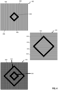
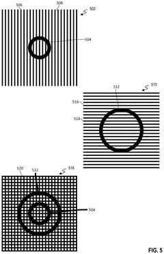
Slit fiducials for integrated circuit device alignment
PatentPendingUS20250006651A1
Innovation
- The use of an array of small alignment marks, specifically slit fiducials with corresponding low-density metal zones, allows for reduced fiducial footprint, smaller low-density metal zones, and improved flexibility in fiducial shape, enabling accurate alignment and reducing fabrication process issues.


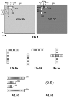
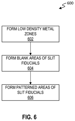
Fiducials with underlying dummy metallization for integrated circuit device alignment
PatentPendingUS20250006652A1
Innovation
- The implementation of low-density metal zones with metal-free slits, which allow for sufficient infrared light passage to determine fiducial locations, enabling precise alignment and reducing fabrication complexities such as CMP and plating issues, while maintaining optical properties regardless of misalignment.
Reliability Testing and Qualification Standards
Reliability testing and qualification standards for heterogeneous integration hybrid bonding have evolved significantly to address the unique challenges posed by this advanced packaging technology. The semiconductor industry has established comprehensive testing protocols that evaluate the mechanical, thermal, and electrical reliability of hybrid bonded interfaces under various stress conditions.
The Joint Electron Device Engineering Council (JEDEC) has developed specific standards for hybrid bonding qualification, including JESD22-A104 for temperature cycling, JESD22-B110 for mechanical shock, and JESD22-A110 for highly accelerated stress testing (HAST). These standards provide structured methodologies to assess bond integrity and long-term reliability performance.
Thermal cycling tests (typically -40°C to 125°C for 1000 cycles) are particularly critical for hybrid bonding reliability assessment, as they simulate the thermal expansion coefficient mismatches between different materials that can induce stress at the bonding interface. The pass criteria generally require less than 1% failure rate after complete testing cycles.
Moisture sensitivity level (MSL) testing has been adapted specifically for hybrid bonded structures, with modified protocols that account for the unique diffusion pathways at the bonding interfaces. This includes extended bake times and specialized inspection techniques to detect moisture-induced delamination or void formation.
Electromigration testing standards have also been enhanced to address the unique current density distributions at hybrid bonded interconnects. The International Reliability Physics Symposium (IRPS) has published guidelines recommending current density stress tests at elevated temperatures (typically 150°C) for 1000+ hours to validate interconnect reliability.
Time-dependent dielectric breakdown (TDDB) testing has emerged as a critical qualification method specifically for hybrid bonding, with specialized test structures designed to evaluate the dielectric integrity between adjacent metal pads. The semiconductor industry typically requires TDDB lifetime projections exceeding 10 years at operating conditions.
Non-destructive evaluation techniques, including scanning acoustic microscopy (SAM) and X-ray computed tomography, have been standardized for in-line and post-reliability testing inspection. These methods allow for void detection and interface quality assessment without compromising the structural integrity of the bonded devices.
The automotive industry has driven the development of more stringent qualification standards for hybrid bonding, with AEC-Q100 Grade 1 requirements extending temperature cycling ranges (-40°C to 150°C) and increasing the number of required cycles to 2000 for mission-critical applications.
Environmental Impact and Sustainability Considerations
Heterogeneous integration hybrid bonding technologies present significant environmental and sustainability implications that must be carefully considered in their development and implementation. The manufacturing processes involved in hybrid bonding typically require substantial energy consumption, particularly during the high-precision alignment and bonding phases, which operate under strictly controlled cleanroom environments.
The chemical processes utilized in surface preparation and bonding activation involve various chemicals including solvents, acids, and specialized cleaning agents. Many of these substances have potential environmental hazards if not properly managed, including contributions to air pollution, water contamination, and hazardous waste generation. Industry leaders are increasingly developing and implementing closed-loop systems for chemical recovery and recycling to mitigate these impacts.
Material selection represents another critical environmental consideration. Traditional semiconductor packaging often relies on lead-based solders and other environmentally problematic materials. Hybrid bonding offers opportunities for more environmentally friendly alternatives by eliminating solder materials entirely, potentially reducing the semiconductor industry's dependence on rare and toxic elements.
From a lifecycle perspective, hybrid bonding technologies may contribute to sustainability through improved device longevity and reliability. The enhanced thermal performance and mechanical stability of hybrid-bonded devices can extend product lifespans, reducing electronic waste generation. Additionally, the higher integration density achievable through hybrid bonding enables smaller form factors, which typically require fewer raw materials and less energy during manufacturing and operation.
Water usage presents a particular sustainability challenge, as semiconductor manufacturing processes, including those for hybrid bonding, are water-intensive. Advanced facilities implementing hybrid bonding technologies must incorporate water recycling systems and efficiency measures to reduce their environmental footprint. Leading manufacturers have reported achieving up to 80% water recycling rates through advanced filtration and purification systems.
Energy efficiency improvements in hybrid bonding equipment and processes are being actively pursued by equipment manufacturers. Next-generation bonding systems incorporate more efficient heating elements, precision cooling systems, and optimized process cycles that significantly reduce energy consumption compared to earlier generation equipment.
Carbon footprint considerations are becoming increasingly important as the semiconductor industry faces pressure to reduce greenhouse gas emissions. Hybrid bonding's potential to enable more energy-efficient devices may partially offset the emissions associated with manufacturing processes, though comprehensive lifecycle assessments are needed to quantify these tradeoffs accurately.
Unlock deeper insights with PatSnap Eureka Quick Research — get a full tech report to explore trends and direct your research. Try now!
Generate Your Research Report Instantly with AI Agent
Supercharge your innovation with PatSnap Eureka AI Agent Platform!