How Heterogeneous Integration Manages Co-Packaged Optics With RF/Power Domains?
SEP 19, 20259 MIN READ
Generate Your Research Report Instantly with AI Agent
Patsnap Eureka helps you evaluate technical feasibility & market potential.
Heterogeneous Integration Background and Objectives
Heterogeneous integration represents a transformative approach in semiconductor packaging, enabling the combination of diverse technologies within a single package. This integration methodology has evolved significantly over the past two decades, transitioning from simple multi-chip modules to sophisticated 2.5D and 3D architectures that combine disparate technologies including digital, analog, RF, photonics, and power management components.
The evolution of heterogeneous integration has been driven by the slowdown of Moore's Law and the increasing demand for higher performance, lower power consumption, and reduced form factors in electronic systems. As traditional silicon scaling faces physical and economic limitations, the industry has pivoted toward advanced packaging solutions to continue performance improvements and functional integration.
In the context of co-packaged optics with RF/power domains, heterogeneous integration addresses the critical challenge of merging high-speed optical communication components with electronic systems. This convergence has become essential as data centers and high-performance computing applications demand unprecedented bandwidth, while simultaneously requiring reduced power consumption and latency.
The technical objectives of heterogeneous integration in this domain are multifaceted. Primary goals include achieving seamless integration of optical engines with electronic ICs, managing thermal interfaces between disparate materials, ensuring signal integrity across high-speed interfaces, and developing reliable manufacturing processes that can scale to high volumes while maintaining economic viability.
Current trends indicate an acceleration toward more complex integration schemes, with particular emphasis on silicon photonics platforms that can be manufactured using modified CMOS processes. These platforms aim to bring optical communication capabilities closer to computing elements, reducing the energy required for data movement and increasing overall system bandwidth density.
The industry is witnessing significant developments in wafer-level and panel-level packaging technologies that enable finer interconnect pitches and higher connection densities between heterogeneous components. Additionally, advances in through-silicon vias (TSVs), interposers, and redistribution layers (RDLs) are creating new possibilities for integrating optics with traditional semiconductor technologies.
Looking forward, heterogeneous integration is expected to continue its trajectory toward greater functional density and performance optimization. The convergence of optical, RF, and power domains within a single package represents not merely an incremental improvement but a paradigm shift in how computing and communication systems are architected and manufactured.
Market Demand for Co-Packaged Optics Solutions
The global market for Co-Packaged Optics (CPO) solutions is experiencing significant growth driven by escalating data center bandwidth demands and the limitations of traditional pluggable optics. Current projections indicate the CPO market will reach approximately $2.3 billion by 2026, with a compound annual growth rate exceeding 35% from 2021 to 2026. This remarkable growth trajectory reflects the urgent need for more efficient data transmission solutions in hyperscale computing environments.
Data center operators face mounting challenges as bandwidth requirements continue to double every two to three years. Traditional pluggable optics architectures struggle to meet these demands due to increasing power consumption, thermal management issues, and physical space constraints. With data rates pushing beyond 400G toward 800G and 1.6T, the electrical-to-optical conversion inefficiencies become increasingly problematic.
The primary market drivers for CPO solutions stem from several converging factors. Power efficiency stands as the foremost concern, with estimates suggesting CPO can reduce power consumption by 30-40% compared to conventional architectures. This translates to substantial operational cost savings for hyperscale data centers, where power represents a significant portion of total operating expenses.
Density requirements constitute another critical market demand. As data centers strive to maximize computational capacity per square foot, CPO's ability to integrate optical components directly with ASICs enables dramatic improvements in port density. Industry benchmarks indicate CPO solutions can achieve up to 2-3 times higher port density compared to traditional pluggable optics implementations.
Latency reduction represents a third key market driver, particularly for high-frequency trading, artificial intelligence training, and other time-sensitive applications. By minimizing the distance between processing and optical components, CPO architectures can reduce signal propagation delays by several nanoseconds – a critical advantage in latency-sensitive environments.
The market demand varies across different industry segments. Hyperscale cloud providers like Amazon, Google, and Microsoft demonstrate the strongest immediate interest, as they operate at scales where the efficiency benefits of CPO translate to substantial cost advantages. Telecommunications providers show growing interest, particularly for edge computing applications where power and space constraints are significant factors. High-performance computing centers represent another promising market segment, driven by the need to minimize latency in tightly coupled computing clusters.
Geographic market distribution reveals North America leading CPO adoption, accounting for approximately 45% of the global market, followed by Asia-Pacific at 35% and Europe at 20%. This distribution largely mirrors the concentration of hyperscale data center deployments and advanced semiconductor manufacturing capabilities.
Technical Challenges in RF/Power Domain Integration
The integration of RF and power domains with co-packaged optics presents significant technical challenges that must be addressed for successful heterogeneous integration. The primary concern is electromagnetic interference (EMI), as RF components generate electromagnetic fields that can disrupt optical signal integrity. This interference becomes particularly problematic in tightly packed heterogeneous systems where optical components require precise signal quality to maintain data transmission reliability.
Thermal management represents another critical challenge, as RF components typically generate substantial heat during operation. Optical components, especially lasers and photodetectors, are highly temperature-sensitive, with performance characteristics that can drift significantly with temperature variations. The thermal gradients created within co-packaged systems can lead to wavelength shifts in optical components, reduced laser efficiency, and increased bit error rates in data transmission.
Signal integrity preservation across domain boundaries requires sophisticated isolation techniques. The transition between RF, electrical power, and optical domains creates potential points of signal degradation that must be carefully managed through specialized interface designs. Traditional approaches using separate packaging for each domain are no longer viable as system integration demands increase.
Power delivery network (PDN) design becomes exceptionally complex in heterogeneous systems. RF components often require clean, stable power supplies with minimal noise, while optical components may have different voltage requirements and sensitivity profiles. The power distribution must maintain isolation between domains while ensuring each component receives appropriate power characteristics without introducing noise into adjacent systems.
Manufacturing challenges are equally significant, as the fabrication processes for RF, power, and optical components differ substantially. RF components typically use specialized substrates optimized for high-frequency performance, while optical components require precise alignment and often utilize materials with different thermal expansion coefficients. Developing unified manufacturing processes that can accommodate these diverse requirements without compromising performance remains difficult.
Testing and validation methodologies must evolve to address the multi-domain nature of these integrated systems. Traditional testing approaches that focus on single domains are insufficient for heterogeneous systems where interactions between domains can create emergent behaviors and failure modes. Comprehensive test strategies must simultaneously evaluate RF performance, optical signal quality, and power integrity across various operating conditions.
Material compatibility issues further complicate integration efforts. Materials optimized for RF performance may not be suitable for optical waveguides or power delivery structures. The selection of materials that can serve multiple functions while maintaining performance across domains represents an ongoing research challenge requiring interdisciplinary expertise.
Current Co-Packaged Optics Integration Approaches
01 System architecture for heterogeneous integration management
Heterogeneous integration management requires specialized system architectures that can handle diverse components and technologies. These architectures provide frameworks for integrating different hardware and software elements, ensuring compatibility and efficient operation. The systems typically include management layers that coordinate between disparate components, enabling seamless communication and operation across heterogeneous environments.- System architecture for heterogeneous integration management: Architectural frameworks designed to manage the integration of diverse hardware and software components in heterogeneous systems. These architectures provide structured approaches for coordinating different technologies, ensuring compatibility, and optimizing performance across integrated systems. The frameworks typically include layered structures that separate concerns while maintaining efficient communication between components.
- Data management in heterogeneous environments: Methods and systems for managing data across heterogeneous platforms, including techniques for data synchronization, transformation, and integration. These solutions address challenges related to data format inconsistencies, varying processing capabilities, and ensuring data integrity across diverse systems. The approaches enable seamless data flow between different components while maintaining consistency and reliability.
- Process integration and workflow management: Techniques for coordinating workflows and processes across heterogeneous systems, ensuring smooth operation and efficient resource utilization. These methods include process scheduling, task allocation, and monitoring mechanisms that optimize the execution of integrated workflows. The solutions enable organizations to manage complex processes spanning multiple technological environments.
- Security and compliance in heterogeneous integration: Security frameworks and compliance mechanisms designed specifically for heterogeneous integrated environments. These solutions address the unique security challenges that arise when integrating diverse systems, including authentication across platforms, secure data transfer, access control, and maintaining regulatory compliance across technological boundaries.
- Performance optimization for heterogeneous systems: Methods for optimizing performance in heterogeneous integrated environments, including resource allocation, load balancing, and system monitoring techniques. These approaches ensure efficient utilization of diverse computing resources while maintaining system stability and responsiveness. The solutions typically involve adaptive algorithms that dynamically adjust resource allocation based on changing workloads and system conditions.
02 Data management in heterogeneous integrated environments
Effective data management is crucial in heterogeneous integrated systems where different data formats, protocols, and storage mechanisms coexist. Solutions include unified data models, cross-platform data exchange protocols, and integration middleware that facilitate seamless data flow between diverse components. These approaches ensure data consistency, integrity, and accessibility across heterogeneous environments while managing the complexity of diverse data structures.Expand Specific Solutions03 Process integration and workflow management
Managing workflows across heterogeneous integrated systems requires specialized approaches to coordinate processes spanning different technological domains. This includes process orchestration tools, workflow engines, and integration frameworks that enable seamless execution of business processes across diverse platforms. These solutions provide mechanisms for process monitoring, exception handling, and optimization in complex heterogeneous environments.Expand Specific Solutions04 Security and compliance in heterogeneous integration
Security management in heterogeneous integrated environments addresses the unique challenges of protecting systems with diverse components and interfaces. This includes unified security frameworks, cross-platform authentication mechanisms, and integrated compliance monitoring. These approaches ensure consistent security policies across heterogeneous components while addressing the specific vulnerabilities that emerge at integration points between different technologies.Expand Specific Solutions05 Performance optimization and resource management
Optimizing performance in heterogeneous integrated systems involves specialized techniques for resource allocation, load balancing, and system monitoring across diverse components. This includes adaptive resource management frameworks, cross-platform performance monitoring tools, and optimization algorithms designed for heterogeneous environments. These approaches ensure efficient utilization of resources while maintaining performance levels across integrated components with different capabilities and characteristics.Expand Specific Solutions
Leading Companies in Heterogeneous Integration
Heterogeneous Integration for Co-Packaged Optics with RF/Power Domains is evolving rapidly in a growth market phase, with the global market expected to reach significant scale by 2025. The technology is approaching early maturity, with key players advancing different integration approaches. TSMC leads in advanced packaging technologies, while Intel and Samsung focus on system-level integration solutions. Research institutions like MIT, Zhejiang Lab, and ITRI are developing next-generation architectures. Companies including Infinera and Unimicron are addressing the critical challenges of thermal management and signal integrity. The industry is moving toward standardization with collaborative efforts between commercial entities and research organizations to overcome the technical barriers of integrating optical, RF, and power domains in compact form factors.
Taiwan Semiconductor Manufacturing Co., Ltd.
Technical Solution: TSMC has pioneered heterogeneous integration for co-packaged optics through their advanced packaging technologies, particularly their Integrated Fan-Out (InFO) and System on Integrated Chips (SoIC) platforms. Their approach focuses on creating high-density interconnects between optical engines, ASICs, and RF components while managing power and thermal domains effectively. TSMC's 3DFabric technology enables the integration of optical I/O with digital processing elements using through-silicon vias (TSVs) and micro-bumps with pitches below 10μm, allowing for extremely compact form factors. Their CoWoS (Chip-on-Wafer-on-Substrate) platform specifically addresses the challenges of integrating optical components with high-performance computing chips, providing thermal isolation between hot digital components and temperature-sensitive optical elements. TSMC has demonstrated successful integration of silicon photonics with CMOS logic, achieving data rates exceeding 100Gbps per channel while maintaining signal integrity across different power domains. Their advanced packaging solutions incorporate specialized power delivery networks that isolate sensitive RF components from digital noise while enabling high-bandwidth optical interconnects.
Strengths: TSMC's mature manufacturing infrastructure enables high-volume production with excellent yield rates. Their advanced node integration capabilities allow for extremely compact designs with optimized power efficiency. Weaknesses: Their solutions may have higher initial NRE costs compared to some competitors, and the thermal management between optical and electrical domains remains challenging in ultra-dense packaging scenarios.
Samsung Electronics Co., Ltd.
Technical Solution: Samsung has developed comprehensive heterogeneous integration solutions for co-packaged optics through their advanced packaging technologies, particularly their X-Cube (eXtended-Cube) and I-Cube (Integration-Cube) platforms. Their approach focuses on 2.5D and 3D integration of optical engines with ASICs and RF components using their through-silicon via (TSV) and hybrid bonding technologies. Samsung's heterogeneous integration platform enables fine-pitch interconnects below 7μm between optical and electrical components, facilitating high-bandwidth, low-latency communication while maintaining separate power domains. Their thermal management solution incorporates embedded silicon interposers with integrated cooling channels that effectively dissipate heat from high-power components while maintaining optimal operating temperatures for sensitive optical elements. Samsung has demonstrated co-packaged optical solutions achieving data rates of 800Gbps with energy efficiency improvements of approximately 40% compared to traditional pluggable optics. Their power management architecture includes dedicated power delivery networks for each domain with specialized isolation techniques to prevent interference between RF signals and optical components. Samsung's advanced packaging also incorporates electromagnetic interference (EMI) shielding structures to protect sensitive optical components from electrical noise.
Strengths: Samsung's vertical integration capabilities from chip manufacturing to advanced packaging enable streamlined production and optimization across the entire supply chain. Their solutions offer excellent scalability for high-volume manufacturing. Weaknesses: Their co-packaged optics solutions may face challenges in standardization across different platforms, and the thermal management between optical and electrical domains requires careful design considerations that may limit some application scenarios.
Key Technologies for RF/Optical Domain Isolation
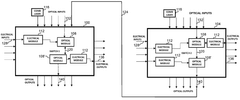
Method and system for co-packaged optics
PatentWO2024236556A1
Innovation
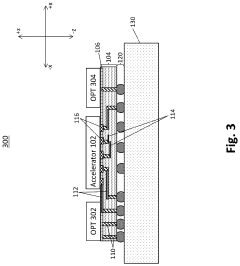
- The laser source is separated from the co-packaged system, with a comb laser serving as an external light source emitting multiple wavelengths, reducing the failure rate and maintenance needs, and used in conjunction with Micro-Ring Modulators and Micro Ring Resonators for bi-directional communication at high transfer rates with low footprint.
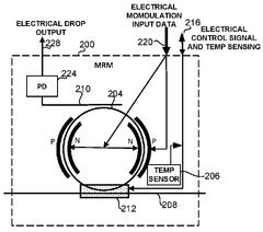
Heterogeneous integration structure with voltage regulation
PatentPendingUS20240215270A1
Innovation
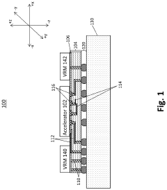
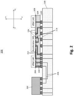
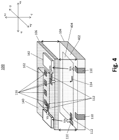
- Incorporating voltage regulator modules (VRMs) on top of the chip, which regulate power from TSVs to processors and memory devices, converting input voltages into operating voltages to compensate for voltage droop and maintain efficient power delivery.
Thermal Management Strategies
Thermal management represents a critical challenge in heterogeneous integration systems that combine co-packaged optics with RF and power domains. The diverse thermal characteristics of these components create complex heat dissipation requirements that must be addressed through comprehensive strategies. Optical components typically have strict temperature tolerances, with lasers and modulators requiring precise thermal control to maintain wavelength stability and performance.
Advanced cooling solutions have emerged as essential elements in managing these thermal challenges. Liquid cooling technologies, including microchannel cold plates and direct liquid cooling, offer superior heat transfer capabilities compared to traditional air cooling methods. These solutions can extract heat more efficiently from high-power-density areas within the integrated package, maintaining optimal operating temperatures across different domains.
Thermal interface materials (TIMs) play a crucial role in establishing effective thermal pathways between components and heat sinks. Recent developments in TIM technology have yielded materials with thermal conductivities exceeding 20 W/mK, significantly improving heat transfer efficiency. Diamond-filled composites and metal-matrix TIMs represent the cutting edge in this field, offering exceptional thermal performance while maintaining necessary electrical isolation properties.
Thermal simulation and modeling have become indispensable tools in the design process of heterogeneous integrated systems. Computational fluid dynamics (CFD) and finite element analysis enable designers to predict hotspots and optimize thermal management strategies before physical prototyping. These simulation approaches account for the complex interactions between optical, RF, and power domains, allowing for more effective thermal design.
Embedded cooling technologies represent another frontier in thermal management for heterogeneous integration. These include integrated microfluidic channels within silicon interposers and vapor chambers embedded directly into package substrates. Such approaches minimize thermal resistance by placing cooling mechanisms closer to heat sources, particularly beneficial for managing the concentrated heat generated by power electronics alongside temperature-sensitive optical components.
Active thermal management techniques, including thermoelectric coolers and phase-change materials, provide dynamic temperature control capabilities essential for optical components. These systems can respond to changing thermal loads during operation, maintaining optimal conditions for temperature-sensitive elements while allowing power components to operate at higher temperatures when necessary.
Manufacturing Scalability and Yield Considerations
Manufacturing scalability and yield considerations represent critical challenges in the heterogeneous integration of co-packaged optics with RF/power domains. The complexity of integrating diverse components—optical engines, electronic ICs, and power delivery systems—into a single package demands sophisticated manufacturing approaches that can maintain high yields while enabling volume production.
Current manufacturing processes for heterogeneous integration face significant yield challenges due to the disparate nature of the components being integrated. Optical components typically require sub-micron alignment precision, while thermal management considerations for power domains add another layer of complexity. Industry data suggests that yield rates for advanced co-packaged optical systems currently hover between 70-85%, significantly lower than the 95%+ yields achieved in conventional semiconductor manufacturing.
The development of standardized manufacturing processes represents a key focus area for improving scalability. Leading manufacturers are investing in advanced assembly equipment capable of handling both optical and electronic components with the required precision. Automated optical alignment systems utilizing machine vision and real-time feedback mechanisms have demonstrated the potential to improve yields by 10-15% in pilot production environments.
Testing methodologies present another critical consideration for manufacturing scalability. Traditional electrical testing approaches must be augmented with optical performance verification, creating a need for integrated test platforms. Several equipment manufacturers have introduced combined electrical-optical test systems that can reduce test time by up to 40% compared to separate testing approaches, thereby enhancing overall manufacturing throughput.
Material selection and compatibility issues further impact manufacturing yields. Thermal expansion mismatches between optical materials, silicon substrates, and power delivery components can lead to stress-induced failures during assembly or reliability testing. Advanced substrate materials with tailored coefficient of thermal expansion (CTE) properties have shown promise in mitigating these issues, with early adopters reporting yield improvements of 5-8%.
Supply chain considerations also play a crucial role in manufacturing scalability. The integration of components from multiple suppliers—optical transceivers, ASICs, power management ICs—requires robust supply chain coordination. Industry consortia are working to establish standardized interfaces and specifications to facilitate interoperability between components from different vendors, potentially reducing integration complexities and associated yield losses.
Looking forward, the industry is exploring advanced packaging technologies such as silicon photonics interposers and glass substrates to improve manufacturing scalability. These approaches aim to reduce the number of critical assembly steps while providing better thermal management capabilities, potentially enabling yield rates above 90% for next-generation co-packaged optical systems.
Unlock deeper insights with Patsnap Eureka Quick Research — get a full tech report to explore trends and direct your research. Try now!
Generate Your Research Report Instantly with AI Agent
Supercharge your innovation with Patsnap Eureka AI Agent Platform!