

How Does Surface Roughness Affect Perovskite Photovoltaics?
AUG 8, 20258 MIN READ
Generate Your Research Report Instantly with AI Agent
PatSnap Eureka helps you evaluate technical feasibility & market potential.
Perovskite PV Evolution
Perovskite photovoltaics have undergone a remarkable evolution since their inception in 2009. The journey began with the groundbreaking work of Tsutomu Miyasaka, who first incorporated perovskite materials into dye-sensitized solar cells. This initial breakthrough, while promising, yielded a modest power conversion efficiency of 3.8%.
The field experienced a significant leap forward in 2012 when Henry Snaith and Michael Grätzel replaced the liquid electrolyte with a solid-state hole transport material. This innovation not only improved stability but also pushed the efficiency to an impressive 10.9%. This development marked the beginning of the rapid ascent of perovskite solar cells in the photovoltaic landscape.
From 2013 to 2016, researchers focused on optimizing the perovskite composition and device architecture. The introduction of mixed-cation and mixed-halide perovskites led to enhanced stability and performance. During this period, efficiencies soared, reaching over 20% by 2015.
The years 2017 to 2019 saw a shift towards addressing the scalability and long-term stability of perovskite solar cells. Researchers began exploring tandem configurations, combining perovskites with silicon or other perovskite layers to push efficiency limits further. By 2019, single-junction perovskite solar cells had achieved certified efficiencies exceeding 25%.
In recent years, from 2020 onwards, the focus has expanded to include environmental concerns and commercialization efforts. Research into lead-free perovskites gained momentum, addressing toxicity issues. Simultaneously, efforts to improve operational stability and develop large-area fabrication techniques intensified.
Throughout this evolution, surface roughness has played a crucial role in device performance. Initially overlooked, its importance became increasingly apparent as efficiencies climbed. Researchers discovered that controlling surface roughness at various interfaces within the device stack could significantly impact charge transport, recombination rates, and overall device stability.
The latest developments in perovskite photovoltaics have seen a convergence of multiple optimization strategies, including precise control over surface morphology. This holistic approach has led to the current record efficiencies exceeding 29% for perovskite-silicon tandem cells, bringing perovskite technology ever closer to commercial viability and widespread adoption in the renewable energy sector.
Market Demand Analysis
The market demand for perovskite photovoltaics has been steadily growing, driven by the increasing global focus on renewable energy sources and the need for more efficient solar technologies. Perovskite solar cells have emerged as a promising alternative to traditional silicon-based photovoltaics due to their potential for higher efficiency, lower production costs, and versatility in applications.
The global solar energy market is projected to experience significant growth in the coming years, with perovskite photovoltaics poised to capture a substantial share. This technology's ability to achieve higher power conversion efficiencies compared to conventional solar cells has attracted considerable attention from both researchers and industry players.
Surface roughness plays a crucial role in the performance of perovskite solar cells, directly impacting their efficiency and stability. As such, there is a growing demand for solutions that can optimize surface roughness in perovskite photovoltaics. This demand is driven by the need to enhance light absorption, reduce recombination losses, and improve overall device performance.
The building-integrated photovoltaics (BIPV) sector has shown particular interest in perovskite technology due to its potential for creating flexible and semi-transparent solar panels. The ability to control surface roughness in perovskite films opens up new possibilities for integrating these solar cells into various architectural designs and structures, further expanding their market potential.
The automotive industry has also expressed interest in perovskite photovoltaics, particularly for electric vehicles. The lightweight nature and potential for high efficiency make perovskite solar cells an attractive option for vehicle-integrated solar panels, provided that surface roughness can be optimized for durability and performance under varying environmental conditions.
In the consumer electronics market, there is a growing demand for portable and wearable devices with integrated solar charging capabilities. Perovskite photovoltaics, with their thin-film nature and potential for flexibility, are well-suited for these applications. However, controlling surface roughness is critical to ensure consistent performance and longevity in such devices.
The aerospace industry has also shown interest in perovskite photovoltaics for satellite and space applications. The lightweight nature and potential for high power-to-weight ratios make perovskite solar cells attractive for these demanding environments, where surface roughness optimization is crucial for maximizing efficiency and durability in the harsh conditions of space.
As the renewable energy sector continues to expand, the demand for advanced manufacturing techniques and materials that can precisely control surface roughness in perovskite photovoltaics is expected to grow. This presents opportunities for companies specializing in nanotechnology, materials science, and advanced manufacturing processes to develop innovative solutions for the perovskite solar cell market.
Surface Roughness Challenges
Surface roughness presents significant challenges in the development and optimization of perovskite photovoltaics. The interface between different layers in a perovskite solar cell plays a crucial role in device performance, and surface roughness directly impacts these interfaces. One of the primary challenges is achieving uniform deposition of subsequent layers when the underlying surface is rough, which can lead to incomplete coverage and the formation of pinholes.
These defects can act as recombination centers, reducing charge carrier collection efficiency and overall device performance. Additionally, rough surfaces can increase light scattering, potentially leading to optical losses and reduced light absorption in the active layer. This is particularly problematic for thin-film perovskite solar cells, where maximizing light absorption within a limited thickness is critical.
Another challenge associated with surface roughness is its impact on charge transport. Rough interfaces can create potential barriers and traps for charge carriers, impeding their efficient extraction and increasing the likelihood of recombination. This effect is especially pronounced at the interface between the perovskite layer and the charge transport layers, where smooth transitions are essential for optimal charge separation and collection.
The presence of surface roughness can also affect the crystallization process of the perovskite layer. Uneven surfaces may lead to non-uniform nucleation and growth of perovskite crystals, resulting in variations in grain size and orientation. This heterogeneity can introduce defects and grain boundaries, which are known to be detrimental to charge transport and overall device stability.
Furthermore, surface roughness can exacerbate degradation processes in perovskite solar cells. Rough surfaces provide more sites for moisture and oxygen ingress, accelerating the decomposition of the perovskite material. This is particularly problematic for long-term stability, as it can lead to faster performance degradation and shorter device lifetimes.
Addressing these challenges requires innovative approaches in materials processing and device fabrication. Techniques such as surface planarization, interface engineering, and the development of self-smoothing materials are being explored to mitigate the negative effects of surface roughness. Additionally, advanced characterization methods are needed to accurately measure and control surface roughness at the nanoscale, enabling more precise optimization of device architectures.
Current Roughness Solutions
01 Surface roughness control in perovskite layers
Controlling the surface roughness of perovskite layers is crucial for improving the performance of perovskite photovoltaic devices. Various techniques are employed to optimize the surface morphology, including solution processing methods, annealing treatments, and the use of additives. These approaches aim to reduce defects, enhance charge transport, and improve overall device efficiency.- Surface roughness control in perovskite layers: Controlling the surface roughness of perovskite layers is crucial for improving the performance of perovskite photovoltaics. Various techniques are employed to optimize the surface morphology, including solution processing methods, annealing treatments, and the use of additives. These approaches aim to reduce defects, enhance charge transport, and improve overall device efficiency.
- Interface engineering for reduced surface roughness: Interface engineering techniques are utilized to reduce surface roughness at the boundaries between different layers in perovskite solar cells. This includes the use of buffer layers, passivation treatments, and selective contact materials. Improved interfaces lead to better charge extraction, reduced recombination losses, and enhanced device stability.
- Nanostructured substrates for controlled perovskite growth: Nanostructured substrates are employed to guide the growth of perovskite films with controlled surface roughness. These substrates can include nanopatterns, textured surfaces, or nanoparticle-based templates. The use of such substrates allows for better control over crystal orientation, grain size, and overall film morphology, leading to improved device performance.
- Post-deposition treatments for surface smoothing: Various post-deposition treatments are applied to smooth the surface of perovskite films. These can include solvent washing, plasma treatments, or mechanical polishing. Such treatments aim to reduce surface roughness, eliminate pinholes, and improve the uniformity of subsequent layer deposition, ultimately enhancing device performance and reproducibility.
- In-situ characterization of surface roughness: Advanced in-situ characterization techniques are developed to monitor and analyze surface roughness during perovskite film formation. These methods include real-time optical monitoring, atomic force microscopy, and spectroscopic ellipsometry. Such techniques enable better understanding and control of the film growth process, leading to optimized surface morphology and improved photovoltaic performance.
02 Interface engineering for reduced surface roughness
Interface engineering techniques are utilized to reduce surface roughness at the boundaries between different layers in perovskite solar cells. This includes the use of buffer layers, passivation treatments, and selective contact materials. By minimizing interfacial defects and improving layer adhesion, these methods contribute to enhanced charge extraction and reduced recombination losses.Expand Specific Solutions03 Nanostructured substrates for controlled perovskite growth
Nanostructured substrates are employed to guide the growth of perovskite films with controlled surface roughness. These substrates can include nanopatterns, textured surfaces, or nanoparticle-decorated layers. By influencing the nucleation and growth processes, these approaches enable the formation of perovskite films with optimized morphology and reduced surface defects.Expand Specific Solutions04 Post-deposition treatments for surface smoothing
Various post-deposition treatments are applied to smooth the surface of perovskite films and reduce roughness. These can include solvent washing, plasma treatments, or mechanical polishing. Such processes aim to eliminate surface irregularities, improve film uniformity, and enhance the interface quality with subsequent layers in the device stack.Expand Specific Solutions05 In-situ monitoring and control of surface roughness
Advanced in-situ monitoring techniques are developed to observe and control surface roughness during perovskite film formation. These methods may involve real-time optical measurements, spectroscopic analysis, or advanced microscopy techniques. By providing immediate feedback on surface morphology, these approaches enable precise control over film growth and optimization of surface properties.Expand Specific Solutions
Key Perovskite PV Players
The surface roughness in perovskite photovoltaics is a critical factor in the competitive landscape of solar energy technology. The industry is in a growth phase, with the global perovskite solar cell market expected to expand significantly in the coming years. While the technology is still maturing, it shows promise for high efficiency and low-cost production. Companies like Oxford Photovoltaics and Trina Solar are at the forefront of commercializing perovskite solar cells, while research institutions such as EPFL and CSEM are driving innovation in surface engineering. The involvement of major players like Toshiba and Panasonic indicates growing interest from established electronics manufacturers, suggesting a shift towards mainstream adoption of perovskite technology in the photovoltaic industry.
Oxford Photovoltaics Ltd.
Technical Solution: Oxford PV has developed a perovskite-on-silicon tandem solar cell technology that addresses surface roughness issues. They use a two-step deposition process for the perovskite layer, which includes spin-coating a lead iodide solution followed by vapor deposition of methylammonium iodide[1]. This method allows for better control of the perovskite crystal growth and surface morphology. They have also implemented advanced surface treatments and interface engineering techniques to minimize recombination losses at the perovskite/silicon interface[2]. Their cells have achieved a record efficiency of 29.52% for perovskite-silicon tandem cells[3], demonstrating the effectiveness of their approach in managing surface roughness effects.
Strengths: High efficiency, scalable manufacturing process, and expertise in tandem cell technology. Weaknesses: Potential challenges in long-term stability and cost-effective large-scale production.
École Polytechnique Fédérale de Lausanne
Technical Solution: EPFL has developed innovative approaches to address surface roughness in perovskite photovoltaics. They have pioneered the use of solution-processed nanocrystalline metal oxide layers as electron transport materials, which can effectively smooth out the underlying surface roughness[4]. Additionally, EPFL researchers have implemented a novel vapor-assisted solution process (VASP) for perovskite deposition, which results in highly uniform and smooth perovskite films with large grain sizes[5]. They have also explored the use of self-assembled monolayers (SAMs) to modify the surface properties of the substrate, improving perovskite crystallization and reducing surface defects[6]. These techniques have led to perovskite solar cells with efficiencies exceeding 25% and improved stability.
Strengths: Cutting-edge research in perovskite materials and interfaces, strong focus on improving stability and efficiency. Weaknesses: Some techniques may be challenging to scale up for commercial production.
Surface Engineering Innovations
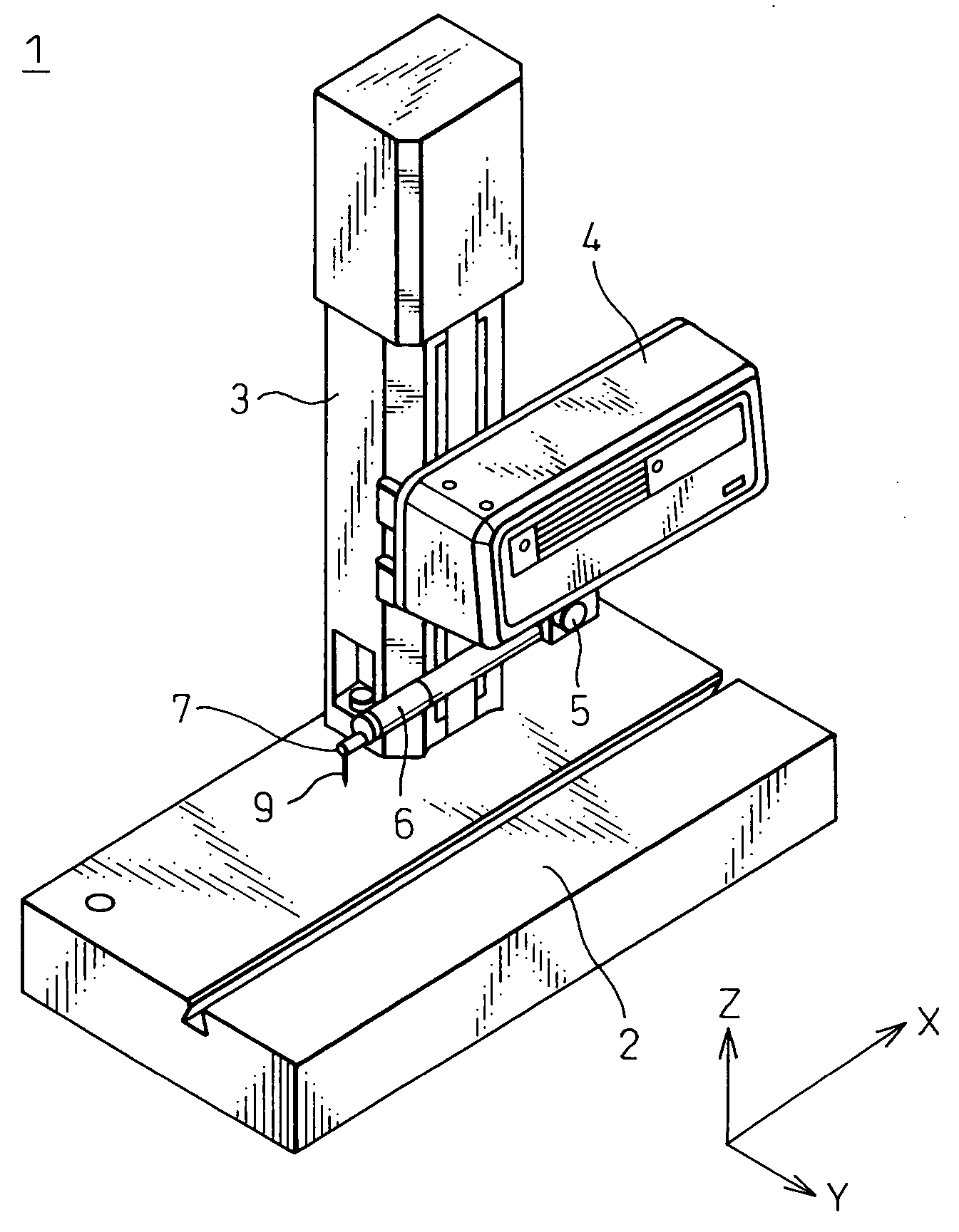
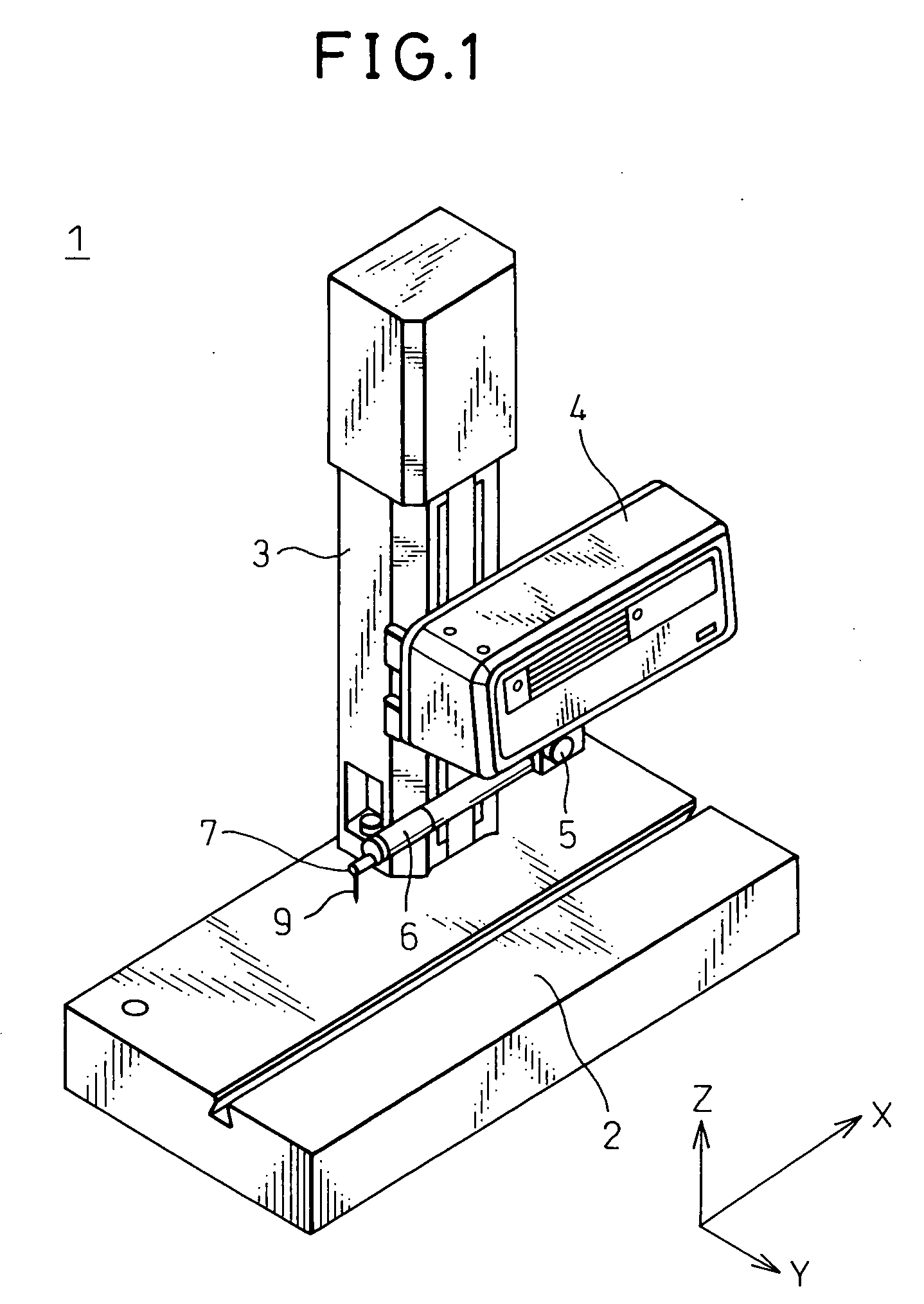
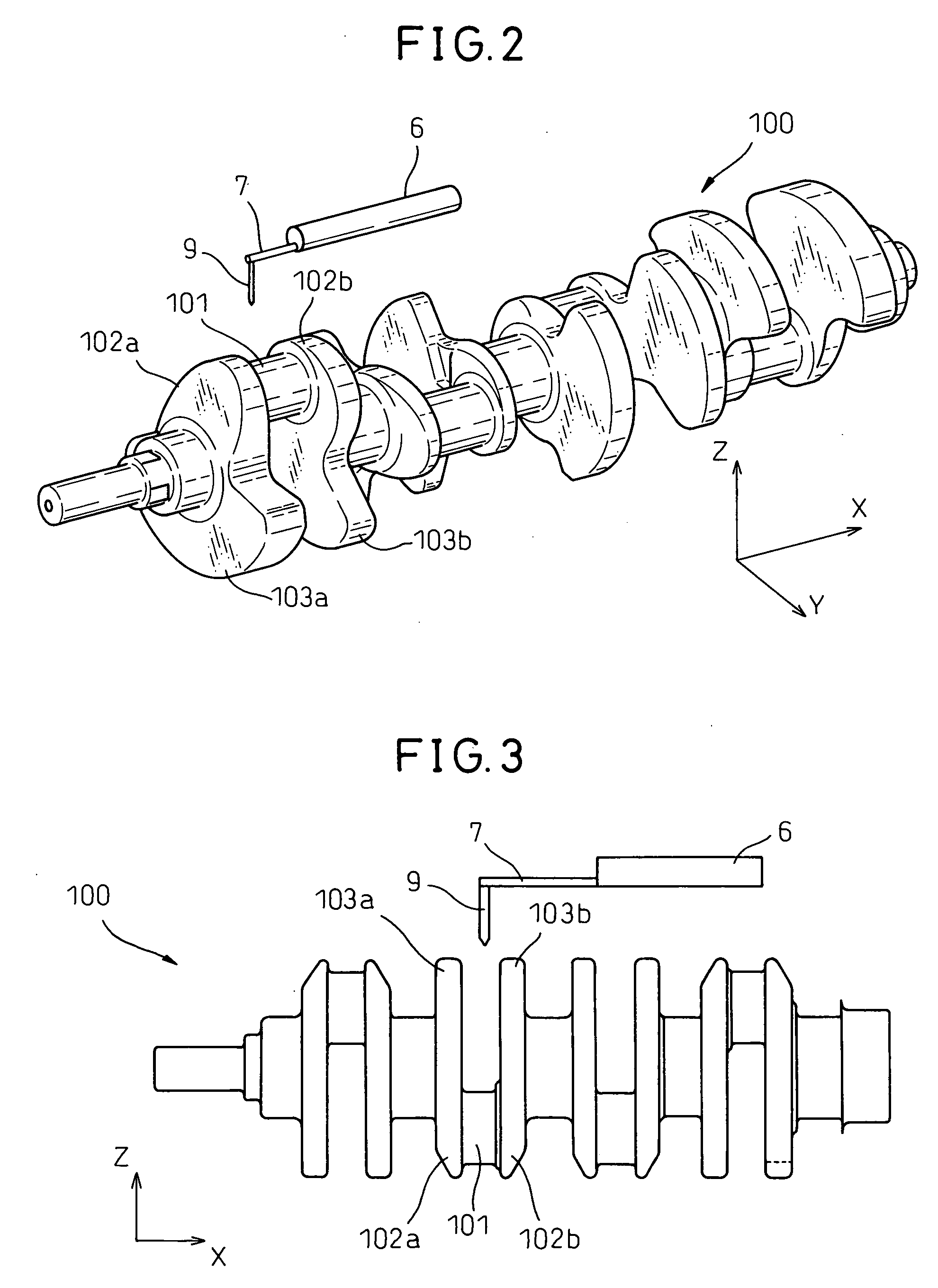
Surface roughness and/or contour shape measuring apparatus
PatentInactiveUS20060249675A1
Innovation
- A surface roughness and contour shape measuring apparatus that moves the probe in directions perpendicular to both its length and the cantilever's length, using a coupling member to facilitate movement and avoid interference with bank portions, allowing for precise measurement of stepped surfaces without requiring a Y-direction drive unit.

Material Characterization
Material characterization plays a crucial role in understanding and optimizing the performance of perovskite photovoltaics, particularly in relation to surface roughness. The surface morphology of perovskite films significantly influences their optoelectronic properties and overall device efficiency.
Atomic Force Microscopy (AFM) is a primary technique used to quantify surface roughness at the nanoscale. It provides high-resolution topographical images and allows for the calculation of root mean square (RMS) roughness values. This data is essential for correlating surface features with device performance metrics.
Scanning Electron Microscopy (SEM) complements AFM by offering a broader view of the film surface. It reveals grain sizes, boundaries, and potential defects that can affect charge transport and recombination processes. Cross-sectional SEM imaging is particularly valuable for examining the interfaces between different layers in the photovoltaic stack.
X-ray Diffraction (XRD) analysis is employed to investigate the crystalline structure of perovskite films. The peak positions and intensities in XRD patterns provide information about crystal orientation and quality, which are influenced by surface roughness and can impact charge carrier dynamics.
Optical characterization techniques, such as UV-Visible spectroscopy and photoluminescence (PL) measurements, are used to assess how surface roughness affects light absorption and emission properties. Rough surfaces can enhance light trapping but may also introduce unwanted scattering or recombination sites.
Time-resolved PL spectroscopy offers insights into charge carrier lifetimes and recombination rates, which can be significantly influenced by surface states and roughness-induced defects. This technique helps in understanding how surface morphology impacts the overall charge dynamics within the perovskite layer.
Surface profilometry provides macroscale roughness measurements, complementing the nanoscale data from AFM. This is particularly useful for assessing the uniformity of large-area perovskite films and identifying potential issues in scalability.
Contact angle measurements are employed to evaluate the wettability of perovskite surfaces, which is crucial for the deposition of subsequent layers in the device structure. Surface roughness can significantly affect wettability and thus impact the quality of interfaces within the photovoltaic stack.
Advanced spectroscopic techniques like X-ray photoelectron spectroscopy (XPS) and ultraviolet photoelectron spectroscopy (UPS) are used to analyze the chemical composition and electronic structure of perovskite surfaces. These methods can reveal how surface roughness influences the distribution of elements and the energetics at the material interfaces.
Scalability Considerations
Scalability considerations are crucial when evaluating the impact of surface roughness on perovskite photovoltaics for large-scale production and deployment. As the technology moves from laboratory-scale devices to commercial applications, the ability to maintain consistent surface properties across larger areas becomes increasingly challenging.
One of the primary concerns in scaling up perovskite solar cell production is the uniformity of the perovskite layer over large areas. Surface roughness plays a significant role in this aspect, as it can affect the nucleation and growth of perovskite crystals. Achieving a uniform surface roughness across large substrates is essential for ensuring consistent device performance and yield in mass production scenarios.
The choice of deposition methods for perovskite layers also becomes more critical when considering scalability. While spin-coating is commonly used in research settings, it may not be suitable for large-scale manufacturing. Alternative techniques such as blade coating, slot-die coating, or spray deposition need to be evaluated for their ability to control surface roughness consistently over larger areas.
Furthermore, the impact of substrate properties on surface roughness becomes more pronounced in large-scale production. Variations in substrate quality or preparation across a large area can lead to inconsistencies in the perovskite layer's surface roughness, potentially affecting device performance and reliability. Developing robust substrate preparation techniques that can be applied uniformly over large areas is essential for scalable production.
The choice of materials and their compatibility with large-scale processing techniques is another important consideration. Some additives or treatments used to control surface roughness in small-scale devices may not be feasible or cost-effective when scaled up. Therefore, research into scalable methods for surface roughness control, such as in-line plasma treatments or solution additives compatible with roll-to-roll processing, is crucial.
Lastly, quality control and characterization methods for surface roughness need to be adapted for large-scale production environments. Developing rapid, non-destructive techniques for measuring and monitoring surface roughness across large areas is essential for maintaining consistent product quality and optimizing production processes. This may involve the use of advanced imaging techniques or inline monitoring systems capable of detecting variations in surface properties during the manufacturing process.
Unlock deeper insights with PatSnap Eureka Quick Research — get a full tech report to explore trends and direct your research. Try now!
Generate Your Research Report Instantly with AI Agent
Supercharge your innovation with PatSnap Eureka AI Agent Platform!