

Antisolvent Engineering in Perovskite Layer Deposition
AUG 8, 20259 MIN READ
Generate Your Research Report Instantly with AI Agent
PatSnap Eureka helps you evaluate technical feasibility & market potential.
Perovskite Antisolvent Evolution and Objectives
Perovskite solar cells have emerged as a promising technology in the field of photovoltaics, with their efficiency rapidly increasing over the past decade. The antisolvent engineering technique has played a crucial role in this development, serving as a key method for depositing high-quality perovskite layers. This approach involves the use of an antisolvent to induce rapid crystallization of the perovskite precursor solution, resulting in improved film morphology and device performance.
The evolution of antisolvent engineering in perovskite layer deposition can be traced back to 2014 when Jeon et al. first introduced the concept. Initially, chlorobenzene was the primary antisolvent used, demonstrating significant improvements in film quality and device efficiency. As research progressed, a wide range of antisolvents were explored, including diethyl ether, toluene, and anisole, each offering unique advantages in terms of perovskite crystallization kinetics and film formation.
The objectives of antisolvent engineering have expanded beyond merely improving film quality. Researchers now aim to achieve precise control over crystal growth, enhance grain size and orientation, reduce defect density, and improve the stability of perovskite films. Additionally, there is a growing focus on developing environmentally friendly and less toxic antisolvent alternatives to address safety concerns associated with traditional organic solvents.
Recent advancements in antisolvent engineering have led to the exploration of mixed antisolvent systems, where two or more solvents are combined to leverage their synergistic effects. This approach has shown promise in fine-tuning the crystallization process and achieving superior film morphology. Furthermore, the integration of additives into antisolvent solutions has emerged as a powerful strategy to passivate defects and enhance the optoelectronic properties of perovskite films.
Looking ahead, the field of antisolvent engineering in perovskite layer deposition is expected to focus on several key objectives. These include developing universal antisolvent systems suitable for a wide range of perovskite compositions, optimizing antisolvent application techniques for large-scale manufacturing, and exploring novel antisolvent materials that can simultaneously improve film quality and long-term stability. Additionally, there is a growing interest in understanding the fundamental mechanisms of antisolvent-induced crystallization through advanced in-situ characterization techniques and computational modeling.
As the perovskite solar cell technology continues to mature, antisolvent engineering will play a vital role in pushing the boundaries of device efficiency and stability. The ultimate goal is to develop scalable and reproducible antisolvent processes that can be seamlessly integrated into industrial-scale production of high-performance perovskite solar modules, paving the way for widespread commercialization of this promising technology.
Market Analysis for Perovskite Solar Cells
The perovskite solar cell market has been experiencing rapid growth and attracting significant attention in recent years. As a promising alternative to traditional silicon-based photovoltaics, perovskite solar cells offer several advantages, including high efficiency, low manufacturing costs, and versatility in applications. The global market for perovskite solar cells is projected to expand substantially over the next decade, driven by increasing demand for renewable energy solutions and advancements in technology.
One of the key factors contributing to the market growth is the continuous improvement in power conversion efficiency (PCE) of perovskite solar cells. Research efforts have led to remarkable progress, with laboratory-scale devices now achieving PCEs exceeding 25%, rivaling the performance of established silicon-based technologies. This rapid efficiency improvement has sparked interest from both academic institutions and commercial entities, fueling further investment in research and development.
The market for perovskite solar cells is segmented based on structure, application, and geography. In terms of structure, planar heterojunction and mesoporous architectures are the primary categories. Applications span a wide range, including building-integrated photovoltaics (BIPV), portable electronics, utility-scale solar farms, and space applications. Geographically, Asia-Pacific, particularly China and South Korea, leads in research output and commercial development, followed by Europe and North America.
Despite the promising outlook, several challenges need to be addressed for widespread commercialization. Stability and durability remain critical concerns, as perovskite materials are sensitive to moisture, heat, and light exposure. Efforts are underway to enhance the long-term stability of these devices through improved encapsulation techniques and material engineering. Additionally, scaling up production from laboratory to industrial scale presents technical and economic hurdles that need to be overcome.
The competitive landscape of the perovskite solar cell market is dynamic, with a mix of established photovoltaic manufacturers, startups, and research institutions. Several companies have announced plans to commercialize perovskite-based products, either as standalone devices or in tandem with silicon cells to boost overall efficiency. Collaborations between academic institutions and industry players are becoming increasingly common, accelerating the transition from lab to market.
Environmental considerations also play a crucial role in market development. While perovskite solar cells offer the potential for lower carbon footprints in manufacturing compared to silicon-based alternatives, concerns about the use of lead in most efficient perovskite formulations have led to research into lead-free alternatives. The success of these efforts could significantly impact market acceptance and regulatory landscapes.
Antisolvent Engineering Challenges
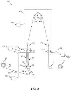
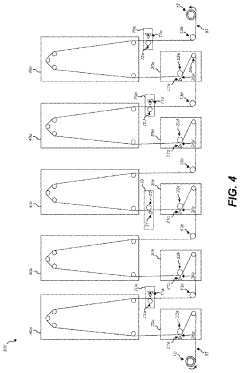
Antisolvent engineering in perovskite layer deposition faces several significant challenges that hinder its widespread adoption and optimization. One of the primary obstacles is the precise control of the antisolvent dripping process. The timing, volume, and uniformity of antisolvent application are critical factors that directly impact the quality and performance of the resulting perovskite film. Even minor variations in these parameters can lead to substantial differences in film morphology, crystallinity, and optoelectronic properties.
Another major challenge lies in the selection of appropriate antisolvents. While commonly used antisolvents like diethyl ether and chlorobenzene have shown promising results, they often present environmental and safety concerns due to their toxicity and high volatility. Finding alternative, eco-friendly antisolvents that can achieve comparable or superior film quality remains an ongoing research focus.
The scalability of antisolvent engineering techniques poses a significant hurdle for industrial-scale production. The current lab-scale methods, which often rely on manual dripping or spin-coating processes, are difficult to translate into large-area, high-throughput manufacturing processes. Developing automated, precise, and uniform antisolvent application methods for large-scale production is crucial for the commercialization of perovskite-based devices.
Furthermore, the sensitivity of perovskite materials to environmental factors such as humidity and temperature adds another layer of complexity to antisolvent engineering. These factors can significantly influence the interaction between the perovskite precursor solution and the antisolvent, affecting the crystallization process and film formation. Maintaining consistent environmental conditions during the deposition process is challenging, especially in large-scale production settings.
The reproducibility and uniformity of perovskite films across large areas remain persistent challenges in antisolvent engineering. Achieving homogeneous film quality over extended surfaces is critical for the fabrication of high-performance, large-area devices. Variations in film thickness, grain size, and defect density across the substrate can lead to inconsistent device performance and reduced overall efficiency.
Lastly, the integration of antisolvent engineering with other deposition techniques and device architectures presents ongoing challenges. Optimizing the antisolvent process to be compatible with various substrate materials, underlying layers, and subsequent processing steps is essential for developing versatile and high-performance perovskite-based devices. This requires a comprehensive understanding of the complex interplay between the antisolvent, perovskite precursors, and other materials in the device stack.
Current Antisolvent Engineering Methods
01 Solution-based deposition methods
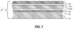
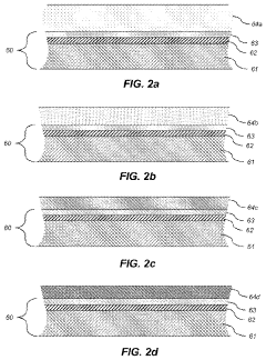
Various solution-based techniques are employed for depositing perovskite layers, including spin-coating, blade coating, and spray coating. These methods offer advantages such as low cost, scalability, and the ability to form uniform thin films. The choice of solvent, concentration, and deposition parameters significantly influence the quality and performance of the resulting perovskite layer.- Solution-based deposition methods: Various solution-based techniques are employed for depositing perovskite layers, including spin-coating, dip-coating, and spray coating. These methods offer advantages such as low-cost processing, scalability, and the ability to form uniform thin films. The choice of solvent, precursor concentration, and deposition parameters significantly influence the quality and performance of the resulting perovskite layer.
- Vapor deposition techniques: Vapor deposition methods, such as thermal evaporation and chemical vapor deposition (CVD), are utilized for perovskite layer formation. These techniques allow for precise control over film thickness and composition, resulting in high-quality perovskite layers with improved crystallinity and reduced defects. Vapor deposition is particularly suitable for fabricating multi-layered perovskite structures and achieving conformal coatings on complex substrates.
- Post-deposition treatments: Various post-deposition treatments are applied to enhance the quality and performance of perovskite layers. These include thermal annealing, solvent annealing, and plasma treatments. Such processes help improve crystallinity, reduce defects, and optimize grain size, leading to better optoelectronic properties and stability of the perovskite layer.
- Additives and composition engineering: Incorporation of additives and composition engineering strategies are employed to enhance the properties of perovskite layers. This includes the use of dopants, passivation agents, and mixed-cation or mixed-halide compositions. These approaches aim to improve stability, charge transport, and optoelectronic properties of the perovskite layer, leading to better device performance and longevity.
- Interface engineering: Interface engineering techniques are applied to optimize the interaction between the perovskite layer and adjacent layers in devices. This includes the use of buffer layers, surface treatments, and selective contact materials. Such strategies aim to reduce interfacial defects, improve charge extraction, and enhance overall device performance and stability.
02 Vapor deposition techniques
Vapor deposition methods, such as thermal evaporation and chemical vapor deposition (CVD), are utilized for perovskite layer formation. These techniques allow for precise control over film thickness and composition, resulting in high-quality perovskite layers with excellent optoelectronic properties. Vapor deposition is particularly useful for creating multi-layered structures and achieving conformal coatings on complex substrates.Expand Specific Solutions03 Post-deposition treatments
Various post-deposition treatments are employed to enhance the quality and performance of perovskite layers. These include thermal annealing, solvent annealing, and plasma treatment. Such processes can improve crystallinity, reduce defects, and optimize the morphology of the perovskite film, leading to better device performance in applications such as solar cells and light-emitting diodes.Expand Specific Solutions04 Compositional engineering
Perovskite layer composition is engineered by incorporating various elements or compounds to enhance stability, efficiency, and optoelectronic properties. This includes the use of mixed cations, halides, and additives. Compositional engineering allows for tuning the bandgap, improving charge transport, and enhancing the overall performance of perovskite-based devices.Expand Specific Solutions05 Interface engineering
Interface engineering techniques are applied to improve the quality of perovskite layers and their integration with other device components. This includes the use of buffer layers, passivation treatments, and surface modifications. These approaches aim to reduce interfacial defects, enhance charge extraction, and improve the overall stability and efficiency of perovskite-based devices.Expand Specific Solutions
Key Players in Perovskite Solar Industry
The antisolvent engineering in perovskite layer deposition field is in a rapidly evolving phase, with significant market growth potential. The technology's maturity is advancing, as evidenced by the involvement of key players like Microquanta, Energy Materials Corp., and Oxford Photovoltaics. These companies are driving innovation in perovskite photovoltaics, focusing on high-efficiency modules and scalable manufacturing processes. The competitive landscape is diverse, including established semiconductor firms like NXP and renewable energy leaders such as LONGi and Hanwha Solutions, alongside specialized perovskite technology developers. This mix of players suggests a dynamic market with opportunities for both breakthrough innovations and industrial scale-up.
Energy Materials Corp.
Technical Solution: Energy Materials Corp. has developed an innovative antisolvent engineering technique for perovskite layer deposition using a roll-to-roll manufacturing process. Their approach involves a continuous deposition method where the perovskite precursor solution is applied to a moving substrate, followed by a carefully timed antisolvent spray[4]. This technique allows for rapid, large-scale production of perovskite solar cells. The company has optimized the antisolvent composition and spray parameters to achieve uniform film formation and high-quality perovskite layers. Their process incorporates in-line drying and annealing steps to further enhance film crystallization and performance[5]. Energy Materials Corp. has demonstrated the ability to produce perovskite solar modules with competitive efficiencies using this scalable manufacturing technique.
Strengths: Enables high-throughput, roll-to-roll production of perovskite solar cells. Potential for significant cost reduction in large-scale manufacturing. Weaknesses: May face challenges in maintaining consistent film quality over large areas compared to batch processes.
LONGi Green Energy Technology Co., Ltd.
Technical Solution: LONGi Green Energy Technology has developed an advanced antisolvent engineering technique for perovskite layer deposition, focusing on large-area, high-efficiency perovskite-silicon tandem solar cells. Their approach involves a modified spin-coating process with a dynamic antisolvent application method[8]. The company has optimized the antisolvent composition, using a blend of chlorobenzene and isopropanol, which is applied in a controlled manner during the spinning process. This technique allows for the formation of uniform, high-quality perovskite films over large areas. LONGi has also incorporated a novel solvent extraction step immediately following the antisolvent application, which helps to remove excess solvent and promote rapid crystallization[9]. This process has enabled the company to achieve high efficiencies in large-area perovskite-silicon tandem solar cells, with reported efficiencies exceeding 26% for modules larger than 100 cm².
Strengths: Enables production of large-area, high-efficiency perovskite-silicon tandem solar cells. Well-suited for integration with existing silicon solar cell manufacturing infrastructure. Weaknesses: May require precise control of multiple parameters during the deposition process, potentially increasing complexity and cost.
Innovative Antisolvent Formulations
Process for producing a layer with mixed solvent system
PatentActiveUS11943993B2
Innovation
- A solvent system comprising a non-polar organic solvent and a first organic amine with at least three carbon atoms is used to solubilize both metal halide perovskite precursor compounds and organic materials, enabling the deposition of crystalline A/M/X materials without toxic solvents and improving film formation.
Method for making a perovskite layer at high speed
PatentActiveUS20240065089A1
Innovation
- A dual solvent system of polar, protic solvents with low boiling points is used for the deposition and drying of perovskite solutions, allowing for high-speed processing at temperatures between 20 to 40 degrees Celsius, with a multi-stage drying process that promotes uniform crystal growth and reduces the need for extensive annealing, thereby enabling the production of defect-free perovskite layers on flexible substrates.
Environmental Impact of Antisolvents
The use of antisolvents in perovskite layer deposition has raised significant environmental concerns due to their potential impact on ecosystems and human health. Many commonly used antisolvents, such as chlorobenzene, toluene, and diethyl ether, are volatile organic compounds (VOCs) that can contribute to air pollution and ozone depletion. These substances may also contaminate soil and water resources if not properly handled and disposed of.
The production and disposal of antisolvents can lead to increased carbon emissions, contributing to global warming and climate change. Furthermore, the manufacturing processes of these chemicals often involve energy-intensive methods and the use of non-renewable resources, exacerbating their environmental footprint.
Exposure to antisolvents can pose health risks to workers in the perovskite solar cell industry. Inhalation of VOCs can cause respiratory irritation, headaches, and in some cases, long-term health effects. This necessitates strict safety protocols and protective equipment in manufacturing facilities.
The accumulation of antisolvent residues in the environment is another concern. These chemicals may persist in ecosystems, potentially affecting wildlife and plant life. Bioaccumulation in food chains could lead to unforeseen consequences for biodiversity and ecosystem balance.
Water pollution is a significant risk associated with antisolvent use. Improper disposal or accidental spills can contaminate groundwater and surface water sources, potentially affecting drinking water supplies and aquatic ecosystems. The treatment of wastewater containing antisolvent residues presents additional challenges and costs for water management systems.
To address these environmental concerns, researchers are exploring greener alternatives to traditional antisolvents. Some promising approaches include the use of non-toxic, biodegradable solvents derived from renewable resources. Additionally, solvent-free or low-solvent deposition techniques are being developed to minimize the reliance on harmful chemicals.
Regulatory bodies are increasingly focusing on the environmental impact of materials used in emerging technologies. This has led to stricter guidelines for the handling, use, and disposal of antisolvents in perovskite solar cell production. Manufacturers are now required to implement more robust waste management and recycling programs to mitigate environmental risks.
The push for sustainability in the solar industry is driving innovation in antisolvent engineering. Researchers are exploring ways to reduce the volume of antisolvents needed in the deposition process, as well as developing closed-loop systems that allow for the recovery and reuse of these chemicals. These efforts aim to create a more environmentally friendly production process for perovskite solar cells, aligning with global sustainability goals.
Scalability of Antisolvent Processes
The scalability of antisolvent processes in perovskite layer deposition is a critical factor for the commercial viability of perovskite solar cells. As the demand for high-efficiency, low-cost photovoltaic technologies continues to grow, the ability to scale up production while maintaining device performance becomes paramount.
Current antisolvent engineering techniques have shown promising results in laboratory settings, typically involving the deposition of small-area devices. However, transitioning these processes to large-scale manufacturing presents several challenges. One of the primary issues is maintaining uniform film quality across larger substrate areas. The rapid crystallization induced by antisolvent treatment can lead to inconsistencies in film morphology and thickness when scaled up.
Another significant challenge is the precise control of antisolvent application over larger areas. In small-scale production, antisolvent is often applied manually or through spin-coating methods. For industrial-scale manufacturing, automated systems for antisolvent deposition must be developed to ensure consistency and repeatability. These systems need to account for factors such as antisolvent volume, droplet size, and application speed to achieve uniform film formation.
The choice of antisolvent also plays a crucial role in scalability. While certain antisolvents may produce high-quality films in small-scale experiments, they may not be suitable for large-scale production due to factors such as cost, toxicity, or volatility. Research into alternative, more environmentally friendly antisolvents that maintain or improve film quality is ongoing.
Substrate size limitations also impact scalability. Many current antisolvent techniques are optimized for small, laboratory-scale substrates. Scaling up to larger substrates requires careful consideration of fluid dynamics, ensuring even distribution of both the perovskite precursor solution and the antisolvent across the entire surface.
Despite these challenges, progress is being made in scaling up antisolvent processes. Some researchers have demonstrated successful antisolvent treatment on substrates up to 100 cm², showing promising results for future industrial applications. Additionally, innovative approaches such as slot-die coating combined with gas-quenching techniques are being explored as potential scalable alternatives to traditional spin-coating methods.
To further improve scalability, ongoing research focuses on optimizing process parameters, developing new antisolvent formulations, and designing advanced deposition equipment. These efforts aim to bridge the gap between laboratory-scale success and commercial-scale production, paving the way for the widespread adoption of perovskite solar cell technology.
Unlock deeper insights with PatSnap Eureka Quick Research — get a full tech report to explore trends and direct your research. Try now!
Generate Your Research Report Instantly with AI Agent
Supercharge your innovation with PatSnap Eureka AI Agent Platform!