

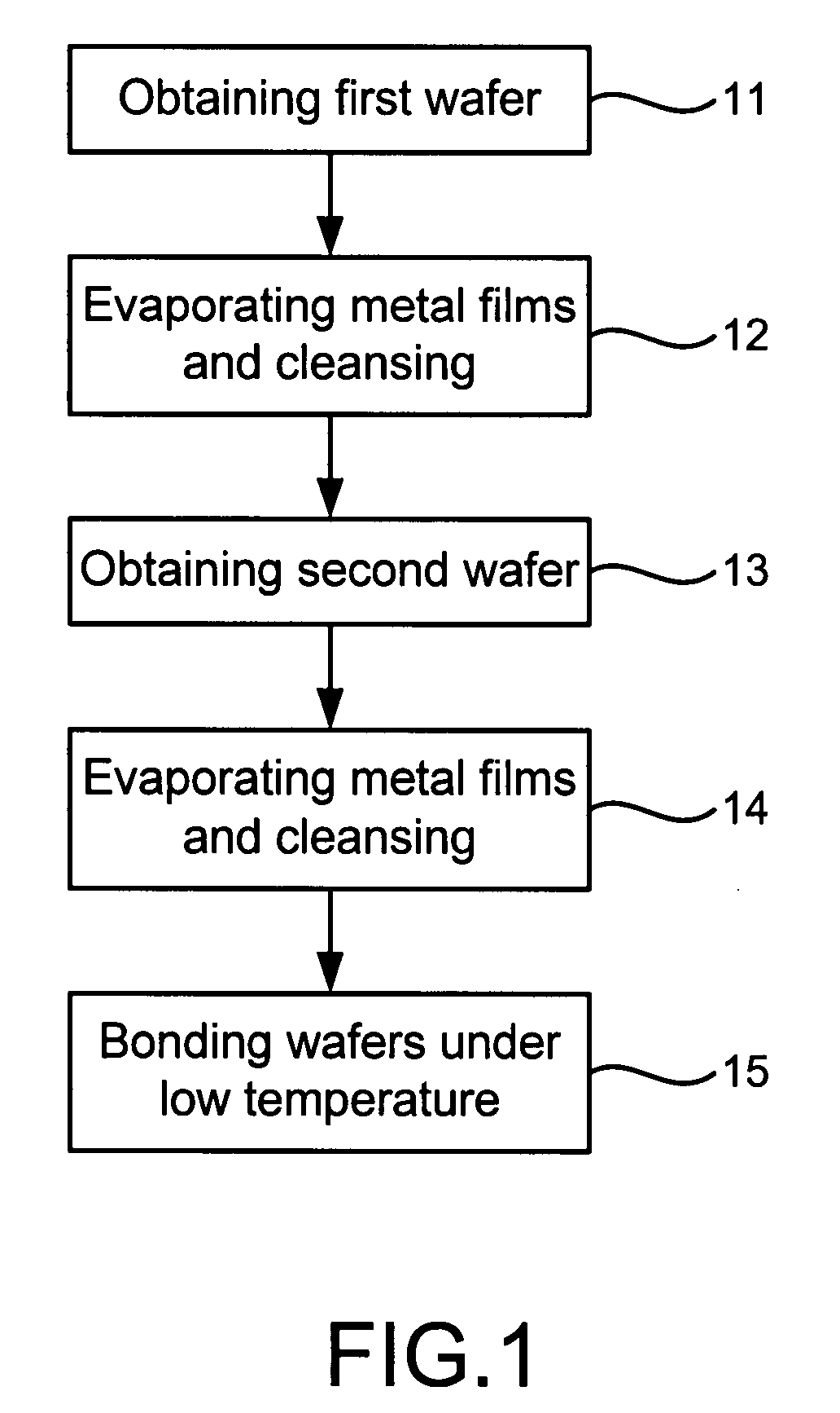
How to Implement Wafer Bonding in Low-Temperature Processes
APR 13, 20269 MIN READ
Generate Your Research Report Instantly with AI Agent
PatSnap Eureka helps you evaluate technical feasibility & market potential.
Low-Temperature Wafer Bonding Background and Objectives
Wafer bonding technology has emerged as a critical enablement technique in advanced semiconductor manufacturing, particularly for three-dimensional integration, MEMS devices, and heterogeneous material integration. Traditional wafer bonding processes typically require elevated temperatures ranging from 800°C to 1200°C, which can introduce thermal stress, material degradation, and compatibility issues with temperature-sensitive components. The evolution toward low-temperature wafer bonding represents a paradigm shift driven by the increasing complexity of modern semiconductor devices and the need for more versatile integration approaches.
The semiconductor industry's relentless pursuit of miniaturization and functional integration has created unprecedented demands for bonding technologies that can operate at temperatures below 400°C, and ideally below 200°C. This temperature reduction is essential for preserving the integrity of pre-fabricated circuits, maintaining the properties of temperature-sensitive materials, and enabling the integration of disparate material systems with different thermal expansion coefficients. Low-temperature processes also reduce energy consumption and manufacturing costs while expanding the range of compatible substrates and device architectures.
The primary objective of implementing low-temperature wafer bonding is to achieve reliable, high-strength bonds between wafer surfaces while maintaining the electrical, mechanical, and thermal properties required for device functionality. This involves developing surface preparation techniques that can create atomically clean and activated surfaces at reduced temperatures, optimizing bonding environments to promote interfacial adhesion, and establishing post-bonding treatments that enhance bond strength without compromising device performance.
Key technical objectives include achieving bond strengths comparable to high-temperature processes, typically exceeding 1 J/m² surface energy, while maintaining void-free interfaces and ensuring long-term reliability under operational conditions. The process must also demonstrate compatibility with existing semiconductor manufacturing infrastructure and maintain throughput requirements for commercial viability.
The strategic importance of low-temperature wafer bonding extends beyond immediate manufacturing benefits to enable entirely new device architectures and applications. This technology facilitates the integration of organic and inorganic materials, enables the fabrication of flexible and stretchable electronics, and supports the development of advanced packaging solutions for next-generation computing and sensing applications. Success in this domain will unlock new possibilities for heterogeneous integration and accelerate innovation across multiple technology sectors.
Market Demand for Low-Temperature Wafer Bonding Solutions
The semiconductor industry is experiencing unprecedented demand for low-temperature wafer bonding solutions, driven by the proliferation of advanced packaging technologies and heterogeneous integration requirements. Traditional high-temperature bonding processes, typically operating above 400°C, pose significant challenges for temperature-sensitive devices and materials, creating substantial market opportunities for innovative low-temperature alternatives.
Advanced packaging applications represent the largest market segment driving this demand. Three-dimensional integrated circuits, system-in-package solutions, and chiplet architectures require precise wafer-level bonding while preserving the integrity of pre-fabricated electronic components. The increasing complexity of semiconductor devices necessitates bonding processes that operate below 200°C to prevent thermal damage to sensitive metallization layers and organic materials.
The MEMS and sensor manufacturing sectors constitute another critical market driver. Pressure sensors, accelerometers, gyroscopes, and biomedical devices often incorporate polymer components, thin-film structures, and delicate mechanical elements that cannot withstand conventional bonding temperatures. Low-temperature processes enable the integration of diverse materials while maintaining dimensional stability and functional performance.
Emerging applications in flexible electronics and wearable devices are expanding market demand significantly. These applications require bonding of substrates with mismatched thermal expansion coefficients, including plastic substrates and ultra-thin silicon wafers. Low-temperature processes minimize thermal stress and prevent warpage, enabling reliable device performance across various form factors.
The photonics industry presents substantial growth opportunities, particularly for silicon photonics and optical interconnect applications. Bonding optical components to electronic substrates requires precise alignment and minimal thermal distortion to maintain optical coupling efficiency. Low-temperature processes preserve the optical properties of waveguides and resonators while enabling high-volume manufacturing.
Market demand is further intensified by sustainability considerations and energy efficiency requirements. Lower processing temperatures reduce energy consumption and carbon footprint, aligning with industry-wide environmental initiatives. Additionally, reduced thermal budgets enable the use of cost-effective substrates and packaging materials, improving overall manufacturing economics.
The automotive electronics sector is driving demand for robust low-temperature bonding solutions capable of withstanding harsh operating environments while maintaining long-term reliability. Power electronics applications require bonding processes that minimize residual stress while ensuring excellent thermal and electrical conductivity.
Current State and Challenges in Low-Temperature Bonding
Low-temperature wafer bonding has emerged as a critical enabling technology for advanced semiconductor manufacturing, particularly in applications requiring temperature-sensitive materials or structures. Current bonding processes typically operate below 400°C, with many applications demanding even lower temperatures under 200°C to preserve the integrity of pre-fabricated devices, metallization layers, and organic materials.
The global landscape of low-temperature bonding technology shows significant regional variations in development focus and capabilities. Leading semiconductor regions including Taiwan, South Korea, Japan, and the United States have established strong research foundations, with European institutions contributing substantially to fundamental bonding mechanisms research. Asian manufacturers dominate production-scale implementations, while North American and European entities lead in specialized applications for MEMS and advanced packaging.
Several fundamental technical challenges continue to constrain widespread adoption of low-temperature bonding processes. Surface preparation requirements become increasingly stringent at reduced temperatures, as lower thermal energy limits the ability to overcome surface contamination and native oxide barriers. Achieving adequate bond strength without high-temperature annealing remains problematic, particularly for direct silicon-to-silicon bonding where typical processes rely on thermal activation for strong covalent bond formation.
Interface quality control presents another significant hurdle, as reduced processing temperatures limit diffusion-based healing of interface defects and voids. This constraint necessitates extremely precise surface preparation and contamination control, driving up process complexity and costs. Additionally, the reduced thermal budget restricts the range of compatible materials and limits the effectiveness of traditional surface activation techniques.
Throughput and scalability challenges further complicate industrial implementation. Many low-temperature bonding approaches require extended processing times or specialized equipment configurations that impact manufacturing efficiency. The need for ultra-clean processing environments and precise parameter control adds operational complexity compared to conventional high-temperature processes.
Current technological gaps include limited understanding of long-term reliability for bonds formed at reduced temperatures, insufficient standardization of process parameters across different material systems, and inadequate metrology techniques for real-time bond quality assessment during low-temperature processing. These limitations collectively represent the primary barriers preventing broader commercial adoption of low-temperature wafer bonding technologies.
Existing Low-Temperature Wafer Bonding Techniques
01 Direct wafer bonding techniques
Direct wafer bonding involves joining two wafers without intermediate layers by bringing atomically clean and flat surfaces into contact. This technique relies on van der Waals forces and can be enhanced through surface activation methods such as plasma treatment or chemical cleaning. The process typically requires precise surface preparation, alignment, and controlled bonding conditions including temperature and pressure. Direct bonding is widely used in MEMS fabrication, 3D integration, and silicon-on-insulator structures.- Direct wafer bonding techniques: Direct wafer bonding involves joining two wafers without intermediate layers by bringing atomically clean and flat surfaces into contact. This technique relies on van der Waals forces and can be enhanced through surface activation methods such as plasma treatment or chemical cleaning. The process typically requires precise surface preparation, alignment, and controlled bonding conditions including temperature and pressure. Direct bonding is widely used for creating silicon-on-insulator structures and three-dimensional integrated circuits.
- Adhesive and intermediate layer bonding: This approach utilizes intermediate materials such as polymers, oxides, or metals between wafer surfaces to facilitate bonding. Adhesive bonding offers advantages including lower temperature requirements, tolerance for surface roughness, and compatibility with different materials. Common intermediate materials include benzocyclobutene, polyimide, and various oxide layers. This method is particularly useful for heterogeneous integration and applications requiring lower thermal budgets.
- Anodic bonding methods: Anodic bonding is an electrochemical process that joins silicon wafers to glass or other materials containing mobile ions. The process involves applying high voltage and elevated temperature, causing ionic migration that creates a strong chemical bond at the interface. This technique is characterized by high bond strength, hermetic sealing capability, and relatively low processing temperatures. It is commonly used in microelectromechanical systems and sensor fabrication.
- Wafer bonding for three-dimensional integration: Three-dimensional wafer bonding enables vertical stacking of multiple device layers to achieve higher integration density and improved performance. This technology involves precise alignment, through-silicon via formation, and specialized bonding techniques to create electrical connections between stacked wafers. The approach addresses challenges including thermal management, mechanical stress, and yield optimization. Applications include high-performance computing, memory devices, and advanced imaging sensors.
- Temporary bonding and debonding processes: Temporary bonding technologies enable wafer processing on both sides by providing temporary mechanical support that can be reversed after processing. These methods use specialized adhesives or bonding materials that can be removed through thermal, chemical, or mechanical means without damaging the device wafer. The technology is essential for thin wafer handling, backside processing, and advanced packaging applications. Key considerations include bond strength during processing, clean debonding, and minimal residue.
02 Adhesive and intermediate layer bonding
This approach utilizes intermediate materials such as polymers, oxides, or metals between wafer surfaces to facilitate bonding. Adhesive bonding offers advantages including lower temperature requirements, tolerance for surface roughness, and compatibility with different materials. Common intermediate materials include benzocyclobutene, polyimide, and various oxide layers. This method is particularly useful when bonding dissimilar materials or when thermal budget constraints exist.Expand Specific Solutions03 Anodic bonding methods
Anodic bonding is an electrochemical process that joins silicon wafers to glass substrates containing mobile ions. The process involves applying high voltage and elevated temperature, causing ion migration and creating a strong permanent bond at the interface. This technique is extensively used in pressure sensors, microfluidic devices, and hermetic packaging applications. The method provides excellent bond strength and hermetic sealing capabilities.Expand Specific Solutions04 Fusion and thermal compression bonding
Fusion bonding employs high temperature and pressure to create atomic-level bonds between wafer surfaces. This process may involve metal layers such as copper or gold that interdiffuse at elevated temperatures to form strong metallurgical bonds. Thermal compression bonding is critical for three-dimensional integrated circuits and advanced packaging technologies. The technique enables high-density interconnections and excellent electrical and thermal conductivity across bonded interfaces.Expand Specific Solutions05 Hybrid and temporary bonding solutions
Hybrid bonding combines multiple bonding mechanisms to achieve specific performance requirements, such as simultaneous dielectric and metal bonding for advanced packaging. Temporary bonding technologies enable processing of thin wafers by providing mechanical support during fabrication, followed by controlled debonding. These approaches address challenges in ultra-thin wafer handling, through-silicon via processing, and heterogeneous integration. The methods incorporate specialized release mechanisms and carrier substrates.Expand Specific Solutions
Key Players in Wafer Bonding Equipment and Materials
The low-temperature wafer bonding technology landscape represents a rapidly evolving sector within the advanced semiconductor packaging industry, currently in its growth phase with significant market expansion driven by 3D integration demands. The market demonstrates substantial scale potential, particularly for applications in CMOS image sensors, memory stacking, and heterogeneous integration. Technology maturity varies significantly across players, with established leaders like Applied Materials and IBM providing comprehensive equipment and process solutions, while specialized companies such as Invensas Bonding Technologies and Adeia Semiconductor Bonding Technologies focus on proprietary bonding methodologies. Asian players including YMTC, SMIC, and Huawei are rapidly advancing their capabilities, supported by strong research institutions like Harbin Institute of Technology and Institute of Microelectronics. The competitive landscape features a mix of equipment manufacturers, foundries, and research organizations, indicating a maturing ecosystem with increasing technological sophistication and commercial viability across diverse application domains.
Invensas Bonding Technologies, Inc.
Technical Solution: Invensas specializes in ZiBond low-temperature direct bonding technology that operates at temperatures as low as 150°C. Their proprietary surface preparation and activation methods enable strong covalent bonds between various materials including silicon, silicon dioxide, and compound semiconductors. The technology incorporates advanced surface cleaning, plasma treatment, and controlled atmosphere bonding processes. ZiBond technology achieves high bond strength and reliability while maintaining compatibility with temperature-sensitive devices and materials, making it suitable for heterogeneous integration and advanced packaging applications.
Strengths: Specialized expertise in low-temperature bonding, proven ZiBond technology platform, strong IP portfolio. Weaknesses: Limited market presence compared to larger equipment manufacturers, dependency on licensing partnerships.
International Business Machines Corp.
Technical Solution: IBM has developed innovative low-temperature wafer bonding techniques focusing on hybrid bonding for advanced semiconductor packaging and 3D chip stacking. Their approach combines surface activation methods with precision alignment systems operating at temperatures below 300°C. IBM's technology enables direct copper-to-copper and dielectric-to-dielectric bonding simultaneously, supporting high-density interconnects for advanced processors and memory devices. The company has demonstrated successful implementation in their advanced node processors, achieving reliable bonds with minimal thermal budget impact on device performance and yield.
Strengths: Strong research capabilities, proven implementation in advanced processors, comprehensive system-level integration expertise. Weaknesses: Limited commercial equipment offerings, focus primarily on internal development rather than external licensing.
Core Innovations in Low-Temperature Bonding Methods
A Method For Low Temperature Bonding Of Wafers
PatentActiveUS20170178929A1
Innovation
- A method involving the use of a first and second wafer with exposed metal layers capable of forming a eutectic mixture, where a predetermined pressure is applied at a temperature below the eutectic melting point to form a solid-state diffusion bond, optionally with a cushioning layer for irregular surfaces, and potentially combining with transient liquid phase bonding for getter activation and multi-chip stacking.


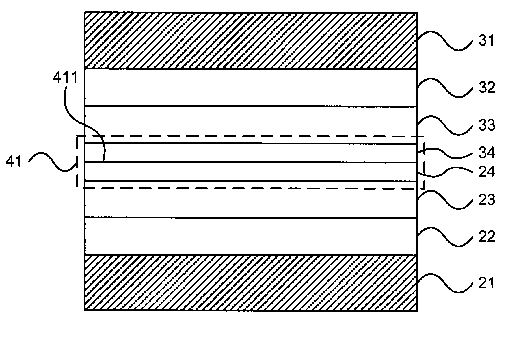
Method of low temperature wafer bonding through Au/Ag diffusion
PatentInactiveUS20080194077A1
Innovation
- A method involving the deposition of Cr, Pt, Au, and Ag films on wafers followed by low-temperature Au/Ag diffusion to form a bonding layer with a melting point above 900°C, reducing thermal stress and enabling robust bonding.

Material Compatibility in Low-Temperature Processes
Material compatibility represents a fundamental consideration in low-temperature wafer bonding processes, where thermal constraints significantly limit the selection of suitable materials and bonding interfaces. The reduced thermal budget, typically below 400°C, necessitates careful evaluation of material properties, thermal expansion coefficients, and chemical interactions to ensure reliable bonding outcomes.
Silicon-based materials demonstrate excellent compatibility in low-temperature processes due to their well-characterized thermal properties and established surface preparation techniques. Silicon dioxide layers, whether thermally grown or deposited via plasma-enhanced chemical vapor deposition, provide reliable bonding interfaces with minimal outgassing and stable chemical composition at reduced temperatures. The compatibility extends to silicon nitride and silicon carbide materials, which maintain structural integrity and exhibit minimal thermal stress during low-temperature bonding cycles.
Metal compatibility becomes increasingly critical as processing temperatures decrease, affecting diffusion rates and intermetallic formation. Copper and aluminum interconnects require careful consideration of their thermal expansion mismatch with silicon substrates. Gold and platinum-based bonding layers demonstrate superior compatibility due to their chemical stability and resistance to oxidation at low temperatures, making them preferred choices for hermetic sealing applications.
Polymer-based materials offer unique advantages in low-temperature processes, with benzocyclobutene, polyimides, and specialized adhesive layers maintaining their bonding properties at reduced thermal budgets. These materials accommodate thermal expansion differences through their inherent flexibility while providing adequate adhesion strength for various applications.
Glass materials, including borosilicate and specialized low-melting-point glasses, present compatibility challenges related to thermal expansion matching and chemical interaction with silicon surfaces. The selection requires precise control of glass composition to minimize stress-induced defects and ensure long-term reliability.
Contamination sensitivity increases significantly in low-temperature processes, as reduced thermal energy limits the ability to drive off surface contaminants and achieve intimate contact between bonding surfaces. Organic residues, moisture, and particulate contamination become more problematic, requiring enhanced surface preparation protocols and controlled ambient conditions during bonding operations.
Quality Control Standards for Low-Temperature Bonding
Quality control standards for low-temperature wafer bonding represent a critical framework ensuring consistent and reliable bonding outcomes while maintaining process integrity at reduced thermal budgets. These standards encompass comprehensive measurement protocols, acceptance criteria, and monitoring procedures specifically tailored to address the unique challenges associated with bonding processes operating below 400°C.
Surface preparation quality control forms the foundation of successful low-temperature bonding. Standards mandate surface roughness measurements with atomic force microscopy, requiring RMS values below 0.5 nm for direct bonding applications. Particle contamination limits are strictly defined, typically allowing no more than 0.1 particles per cm² for particles larger than 0.2 μm. Chemical cleanliness verification through contact angle measurements and surface energy analysis ensures optimal bonding interface conditions.
Bonding uniformity assessment requires standardized void detection methodologies using acoustic microscopy or infrared imaging. Acceptable void density thresholds are established based on application requirements, commonly limiting void coverage to less than 1% of the total bonded area. Bond strength evaluation protocols specify minimum pull-test values and die shear strength requirements, with typical acceptance criteria ranging from 10-50 MPa depending on the specific bonding technique employed.
Temperature and pressure monitoring during the bonding process demands calibrated instrumentation with documented traceability. Process control charts track critical parameters including temperature uniformity across the wafer surface, pressure distribution, and ambient atmosphere composition. Statistical process control methods identify process drift and establish control limits for key variables affecting bond quality.
Post-bonding characterization standards define inspection protocols for interface integrity assessment. Cross-sectional analysis requirements specify sample preparation methods and evaluation criteria for interface defects, delamination, and material interdiffusion. Electrical testing standards for bonded structures include contact resistance measurements and isolation verification between bonded layers.
Documentation requirements ensure complete traceability throughout the bonding process. Quality control records must capture pre-bonding surface conditions, process parameters, real-time monitoring data, and post-bonding inspection results. Statistical analysis of quality metrics enables continuous process improvement and yield optimization while maintaining compliance with industry standards and customer specifications.
Unlock deeper insights with PatSnap Eureka Quick Research — get a full tech report to explore trends and direct your research. Try now!
Generate Your Research Report Instantly with AI Agent
Supercharge your innovation with PatSnap Eureka AI Agent Platform!