

How To Optimize Clamp Release Timing For Electrostatic Chuck Systems
MAY 14, 20268 MIN READ
Generate Your Research Report Instantly with AI Agent
PatSnap Eureka helps you evaluate technical feasibility & market potential.
Electrostatic Chuck Clamp Release Background and Objectives
Electrostatic chuck (ESC) systems have emerged as critical components in semiconductor manufacturing processes, particularly in plasma etching, ion implantation, and chemical vapor deposition applications. These systems utilize electrostatic forces to securely hold wafers during processing, eliminating the need for mechanical clamping mechanisms that could introduce contamination or damage. The evolution of ESC technology has been driven by the semiconductor industry's relentless pursuit of smaller feature sizes, higher precision, and improved yield rates.
The fundamental principle of electrostatic chucking relies on creating strong attractive forces between a dielectric surface and the wafer through applied voltage. However, the release mechanism presents unique challenges that have become increasingly complex as wafer sizes have grown and process requirements have become more stringent. Traditional release methods often result in wafer sticking, non-uniform release patterns, or potential wafer damage due to improper timing sequences.
Historical development of ESC systems began in the 1980s with simple monopolar designs, progressing through bipolar configurations in the 1990s, and evolving into sophisticated multi-zone systems in the 2000s. Each generation has brought improvements in clamping force uniformity and temperature control, yet the release timing optimization has remained a persistent challenge requiring continuous innovation.
The primary objective of optimizing clamp release timing centers on achieving rapid, uniform, and damage-free wafer release while maintaining process throughput requirements. This involves developing precise control algorithms that account for residual charge dissipation, surface adhesion forces, and environmental factors such as temperature and humidity variations.
Current technological goals focus on implementing intelligent release sequences that can adapt to different wafer types, process histories, and chamber conditions. Advanced objectives include developing predictive models that can anticipate optimal release timing based on real-time monitoring of electrostatic forces and surface conditions.
The ultimate aim is to establish industry-standard protocols for release timing optimization that can reduce wafer breakage rates below 0.001%, minimize release time to under 5 seconds, and ensure consistent performance across varying operational conditions while supporting next-generation semiconductor manufacturing requirements.
Market Demand for Advanced ESC Systems
The semiconductor manufacturing industry is experiencing unprecedented growth driven by expanding applications in artificial intelligence, 5G communications, automotive electronics, and Internet of Things devices. This surge in demand has created substantial market pressure for advanced electrostatic chuck systems that can deliver superior wafer handling precision and reliability. Modern semiconductor fabrication facilities require ESC systems capable of processing larger wafer sizes, handling more delicate materials, and maintaining tighter process control specifications.
Advanced ESC systems with optimized clamp release timing capabilities are becoming critical differentiators in high-volume manufacturing environments. The market demand stems from the need to minimize wafer breakage, reduce particle contamination, and improve overall equipment effectiveness. Semiconductor manufacturers are increasingly prioritizing ESC solutions that can seamlessly integrate with automated wafer handling systems while maintaining consistent performance across extended production cycles.
The automotive semiconductor segment represents a particularly strong growth driver for advanced ESC technology. Electric vehicle adoption and autonomous driving systems require specialized semiconductor components that demand precise manufacturing processes. These applications necessitate ESC systems with enhanced clamp release control to handle power semiconductors and sensor components that are often more fragile than traditional logic chips.
Memory and storage device manufacturing also contributes significantly to ESC market demand. The transition to advanced memory architectures such as 3D NAND and emerging storage class memory technologies requires sophisticated wafer processing capabilities. Manufacturers in this segment seek ESC systems that can accommodate varying substrate thicknesses and material compositions while maintaining optimal clamp release timing across different process steps.
Equipment manufacturers are responding to market demands by developing ESC systems with intelligent clamp release algorithms and real-time monitoring capabilities. The integration of advanced sensors and machine learning technologies enables predictive maintenance and process optimization, addressing customer requirements for higher uptime and reduced total cost of ownership. This technological evolution reflects the market's shift toward smart manufacturing solutions that can adapt to varying production requirements while maintaining consistent quality standards.
Current ESC Clamp Release Challenges and Limitations
Electrostatic chuck systems face significant challenges in achieving optimal clamp release timing, primarily due to the complex nature of electrostatic forces and residual charge effects. The fundamental issue lies in the unpredictable behavior of residual charges that remain trapped within the dielectric layer after power disconnection. These charges create persistent attractive forces between the wafer and chuck surface, leading to inconsistent release timing and potential wafer handling complications.
Temperature variations present another critical limitation affecting clamp release performance. As processing temperatures fluctuate during semiconductor manufacturing cycles, the dielectric properties of ESC materials change substantially. Higher temperatures typically reduce dielectric strength and alter charge dissipation rates, while lower temperatures can increase charge retention time. This temperature dependency makes it extremely difficult to predict and control release timing across different process conditions.
Surface contamination and particle accumulation on chuck surfaces create additional complications for release timing optimization. Microscopic particles and residual process chemicals can alter local electric field distributions, creating non-uniform charge dissipation patterns. These contamination effects result in partial wafer adhesion, where some areas release properly while others maintain strong electrostatic attraction, potentially causing wafer damage during handling operations.
The inherent material properties of different wafer types and backside coatings introduce further variability in release characteristics. Silicon wafers with various doping levels, compound semiconductors, and wafers with specialized backside films each exhibit unique electrical properties that affect charge accumulation and dissipation behavior. This diversity requires adaptive release strategies that current ESC systems struggle to accommodate effectively.
Process-induced charging effects from plasma exposure and ion bombardment significantly complicate release timing control. During plasma processing, wafers accumulate substantial surface charges that interact with ESC electrostatic fields in unpredictable ways. These process-induced charges can either enhance or oppose the clamping force, making it challenging to determine appropriate release timing parameters.
Current ESC control systems lack sophisticated real-time monitoring capabilities to assess actual clamping force levels and charge distribution states. Most systems rely on predetermined timing sequences rather than dynamic feedback control, resulting in either insufficient release time leading to wafer sticking, or excessive release time reducing throughput efficiency. The absence of integrated force sensing and charge measurement technologies limits the ability to implement intelligent release timing optimization strategies.
Existing Clamp Release Timing Solutions
01 Timing control mechanisms for electrostatic chuck release
Systems that incorporate precise timing control mechanisms to manage the release sequence of electrostatic chucks. These mechanisms ensure proper coordination between the clamping force reduction and substrate release, preventing damage during wafer handling operations. The timing control can be implemented through electronic controllers that monitor various process parameters and execute release sequences at optimal moments.- Timing control mechanisms for electrostatic chuck release: Systems that implement precise timing control mechanisms to manage the release sequence of electrostatic chucks. These mechanisms ensure proper coordination between the clamping force reduction and substrate release, preventing damage during wafer handling operations. The timing control can be achieved through electronic controllers that monitor various parameters and execute predetermined release sequences.
- Voltage discharge control for clamp release: Methods for controlling the voltage discharge process during electrostatic chuck release operations. These systems manage the rate and sequence of voltage reduction to ensure safe and controlled release of clamped substrates. The discharge control prevents sudden release that could cause substrate movement or damage, while maintaining process reliability.
- Multi-zone release coordination systems: Advanced electrostatic chuck systems that coordinate the release timing across multiple zones or electrodes. These systems enable selective or sequential release of different areas of the substrate, providing enhanced control over the release process. The multi-zone approach allows for optimized substrate handling and reduced risk of substrate warping or breakage.
- Feedback-based release timing optimization: Systems that utilize feedback mechanisms to optimize the timing of electrostatic chuck release operations. These implementations monitor substrate conditions, environmental factors, or system parameters to dynamically adjust release timing for optimal performance. The feedback control ensures consistent release behavior across different operating conditions and substrate types.
- Safety interlocks and emergency release protocols: Safety systems that implement interlocks and emergency release protocols for electrostatic chuck operations. These systems provide fail-safe mechanisms to ensure proper release timing even under abnormal conditions or system failures. The safety protocols include emergency discharge sequences and backup timing controls to prevent substrate damage or equipment malfunction.
02 Voltage discharge control for clamp release
Methods for controlling the voltage discharge process during electrostatic chuck release operations. These systems manage the rate and sequence of voltage reduction to ensure safe and controlled substrate release. The discharge control prevents sudden release that could cause substrate movement or damage, while maintaining process efficiency through optimized discharge timing patterns.Expand Specific Solutions03 Multi-zone release coordination systems
Electrostatic chuck systems that feature multiple zones with independent release timing control. These systems allow for sequential or simultaneous release of different chuck zones based on process requirements. The coordination between zones ensures uniform substrate release and prevents warping or stress concentration during the unclamping process.Expand Specific Solutions04 Sensor-based release timing optimization
Systems that utilize various sensors to determine optimal release timing for electrostatic chucks. These sensors monitor parameters such as substrate position, temperature, and electrostatic force levels to automatically adjust release timing. The sensor feedback enables adaptive control that responds to varying process conditions and substrate characteristics for improved handling reliability.Expand Specific Solutions05 Safety interlocks and emergency release protocols
Safety systems designed to handle emergency situations and provide fail-safe release mechanisms for electrostatic chucks. These protocols include backup power systems, manual override capabilities, and automatic release triggers activated by abnormal conditions. The safety interlocks ensure substrate and equipment protection while maintaining operator safety during unexpected events or system failures.Expand Specific Solutions
Key Players in ESC and Semiconductor Equipment Industry
The electrostatic chuck (ESC) clamp release timing optimization market represents a mature yet evolving segment within semiconductor manufacturing equipment. The industry is in an advanced development stage, driven by increasing demands for precision wafer handling in sub-7nm processes. Market size reflects the broader semiconductor equipment sector's growth, valued at approximately $100+ billion globally. Technology maturity varies significantly among key players: established leaders like Applied Materials, Tokyo Electron, and Lam Research demonstrate high technical sophistication with proven ESC solutions, while Taiwan Semiconductor Manufacturing Company and GlobalFoundries drive demand-side innovation. Beijing NAURA and other emerging players are rapidly advancing their capabilities. The competitive landscape shows consolidation around companies with deep process control expertise, advanced materials science capabilities, and integrated system solutions that can precisely manage electrostatic forces during wafer release cycles for optimal yield performance.
Beijing NAURA Microelectronics Equipment Co., Ltd.
Technical Solution: Beijing NAURA has developed clamp release timing optimization technology for their plasma processing equipment, focusing on cost-effective solutions for emerging semiconductor markets. Their system incorporates basic sensor feedback mechanisms to monitor chuck voltage decay and substrate temperature during release cycles. The technology uses simplified control algorithms that balance performance with system complexity, making it suitable for applications where cost considerations are important. Their approach includes preset timing profiles optimized for common substrate materials and process conditions, with manual adjustment capabilities for specific applications. The system features basic data logging and analysis tools that help operators optimize timing parameters based on process requirements and equipment performance characteristics.
Strengths: Cost-effective solutions, growing market presence in Asia, focus on practical implementation for emerging markets. Weaknesses: Limited advanced features compared to established competitors, smaller installed base for data collection and algorithm refinement.
Lam Research Corp.
Technical Solution: Lam Research has implemented intelligent clamp release timing optimization in their etch and deposition systems through their Sense.i platform. Their approach utilizes machine learning algorithms to analyze historical process data and predict optimal release timing based on process parameters such as RF power levels, gas chemistry, and substrate temperature profiles. The system incorporates advanced sensors that monitor chuck capacitance changes and voltage decay characteristics in real-time. Their technology features adaptive timing control that automatically adjusts release sequences based on wafer bow measurements and stress analysis. The platform includes predictive maintenance capabilities that optimize timing parameters to extend chuck lifetime while maintaining process reliability and yield performance.
Strengths: Strong expertise in plasma processing equipment, advanced data analytics capabilities, excellent integration with existing process tools. Weaknesses: Limited to specific process applications, requires significant data collection period for optimal performance.
Core Patents in ESC Release Optimization
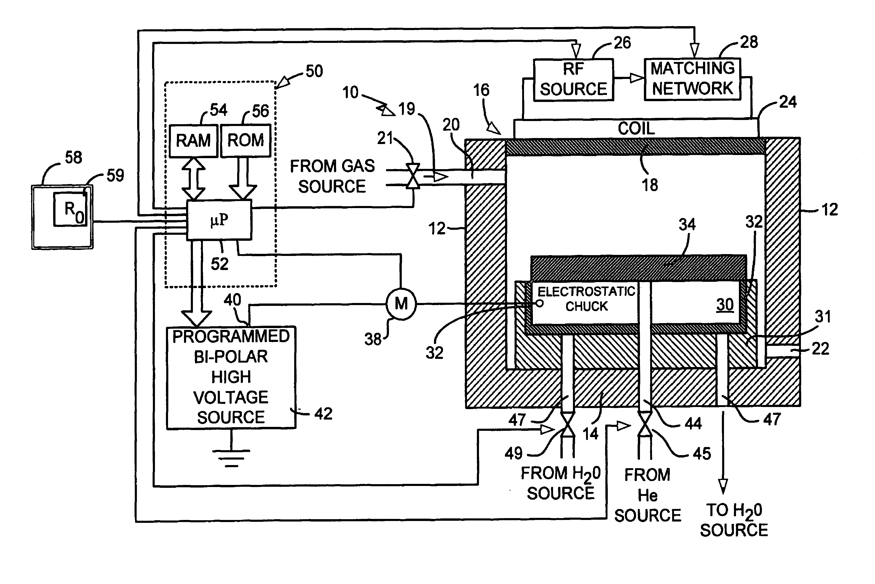
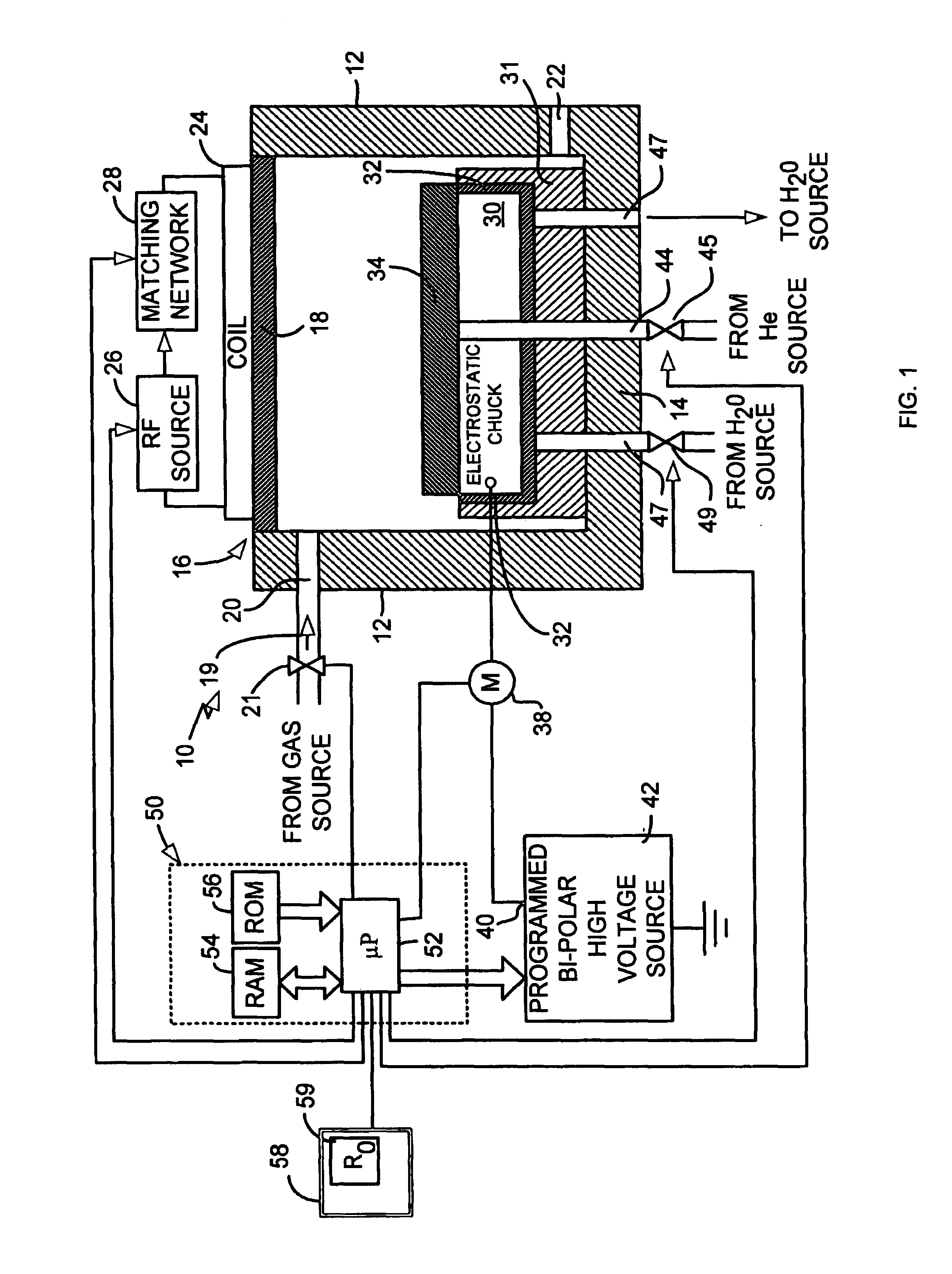
System and method for dechucking a workpiece from an electrostatic chuck
PatentInactiveUS6965506B2
Innovation
- A system and method that uses a microprocessor to generate correlations between ESC electrical properties and dechucking parameters, involving a single experimental test to calculate a fitting parameter, allowing for predictive modeling of dechucking parameters that consider temperature and unique ESC properties, and automatically adjusts dechucking voltage and time to minimize current spikes during the dechucking process.
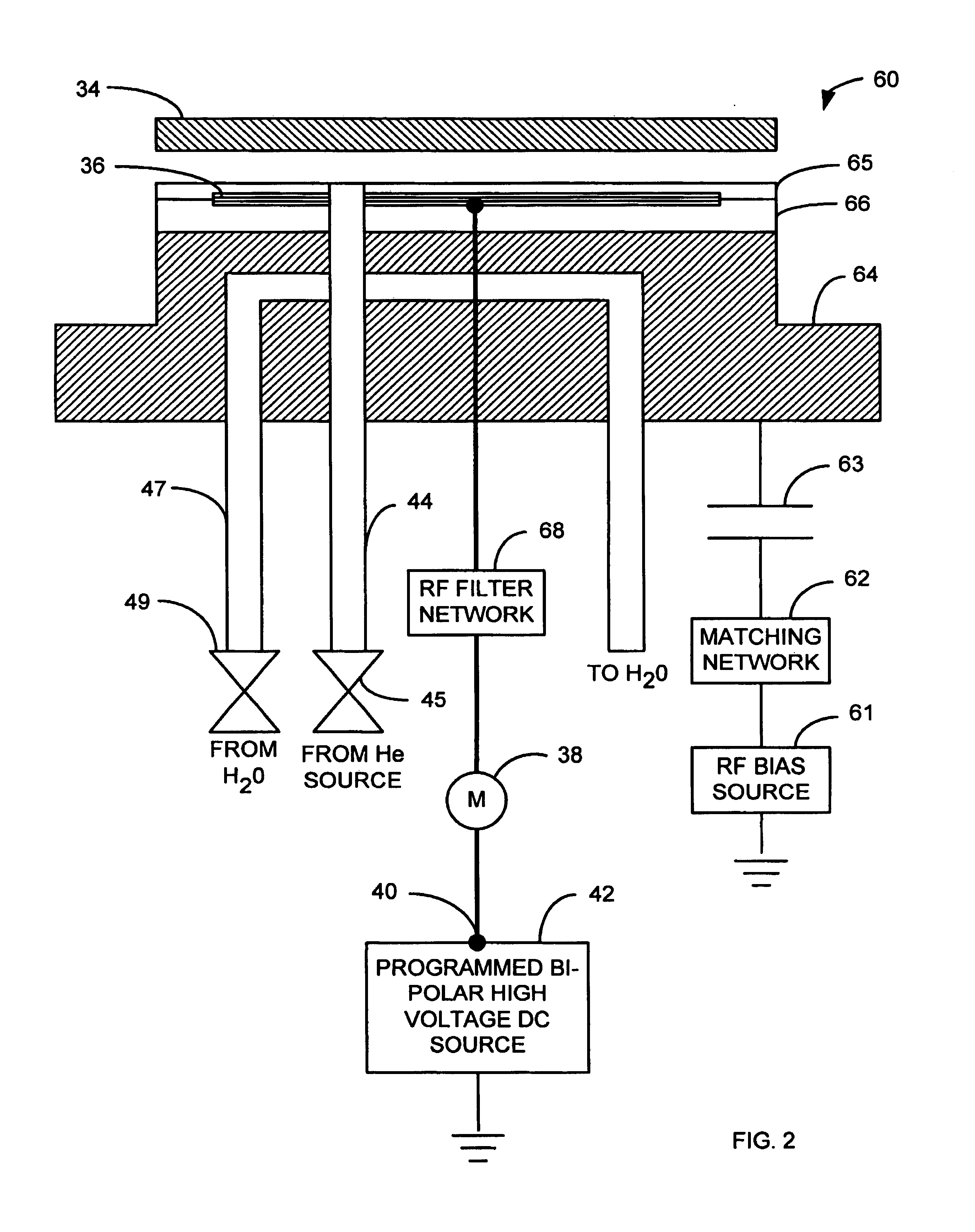

Step down dechucking
PatentActiveUS8164879B2
Innovation
- A method involving a multi-stage process where the electrostatic chucking voltage is gradually reduced and then increased to control the escape of gas, ensuring the repulsive force from residual gas is less than the attractive force, allowing for controlled wafer release without damage.


Safety Standards for ESC Systems
Safety standards for electrostatic chuck (ESC) systems represent a critical framework governing the secure operation of these precision semiconductor manufacturing tools. The primary regulatory bodies establishing these standards include SEMI (Semiconductor Equipment and Materials International), IEC (International Electrotechnical Commission), and various national safety organizations. These standards specifically address high-voltage electrical safety, personnel protection protocols, and equipment reliability requirements that directly impact clamp release timing optimization.
The fundamental safety requirements for ESC systems encompass electrical isolation standards, typically mandating minimum dielectric strength of 5kV between high-voltage electrodes and grounded components. Personnel safety protocols require comprehensive lockout/tagout procedures during maintenance operations, with specific emphasis on discharge timing sequences that must be coordinated with clamp release mechanisms. Emergency shutdown systems must be capable of safely releasing wafers within specified timeframes while maintaining electrical safety margins.
Clamp release timing optimization must comply with SEMI S2 and S8 safety guidelines, which establish maximum allowable voltage decay rates and minimum discharge verification periods. These standards require that ESC systems incorporate redundant safety interlocks preventing premature wafer release during active clamping cycles. The timing optimization algorithms must integrate safety monitoring functions that continuously verify proper electrode discharge before initiating mechanical release sequences.
Environmental safety considerations include electromagnetic interference (EMI) compliance per FCC Part 15 and CE marking requirements, ensuring that optimized timing control systems do not generate harmful electromagnetic emissions. Cleanroom compatibility standards mandate that all safety systems operate reliably in controlled atmospheric conditions while maintaining particle generation limits below specified thresholds.
Recent updates to safety standards emphasize predictive safety monitoring, requiring ESC systems to implement real-time diagnostics that can detect potential timing anomalies before they compromise wafer handling safety. These enhanced requirements necessitate sophisticated control algorithms capable of adapting release timing parameters while maintaining strict adherence to established safety boundaries and operational reliability standards.
Process Integration Considerations for ESC Optimization
Process integration considerations for ESC optimization represent a critical dimension in semiconductor manufacturing where clamp release timing must harmonize with upstream and downstream fabrication processes. The integration challenges extend beyond isolated chuck performance to encompass thermal cycling compatibility, contamination control protocols, and throughput optimization across multiple process chambers.
Thermal management integration poses significant constraints on clamp release timing optimization. The electrostatic chuck must coordinate with chamber temperature control systems, ensuring that wafer release occurs within acceptable thermal gradients to prevent substrate warping or stress-induced defects. Process integration requires careful synchronization between ESC cooling cycles and subsequent handling operations, particularly when transitioning between high-temperature processes such as plasma etching or chemical vapor deposition.
Contamination control protocols directly influence clamp release timing parameters within integrated process flows. The release sequence must accommodate particle removal procedures, backside gas purging, and chamber conditioning steps that maintain cleanroom standards. Integration with automated wafer handling systems necessitates precise timing coordination to minimize exposure periods while ensuring complete electrostatic discharge and particle mitigation.
Throughput optimization demands that ESC clamp release timing aligns with overall equipment effectiveness metrics across the fabrication line. Process integration considerations include minimizing dwell times between process steps, optimizing chamber utilization rates, and reducing wafer handling bottlenecks. The release timing must balance rapid throughput requirements against process quality constraints, particularly in high-volume manufacturing environments where cycle time reductions directly impact production economics.
Multi-chamber tool integration presents additional complexity where ESC optimization must consider wafer state transitions between different process environments. The clamp release timing affects wafer temperature stabilization, surface conditioning, and preparation for subsequent process steps. Integration protocols must account for varying process requirements across different chambers while maintaining consistent wafer handling performance and minimizing cross-contamination risks between process modules.
Unlock deeper insights with PatSnap Eureka Quick Research — get a full tech report to explore trends and direct your research. Try now!
Generate Your Research Report Instantly with AI Agent
Supercharge your innovation with PatSnap Eureka AI Agent Platform!