How To Optimize Electrostatic Chucks For Wafer Alignment
MAY 14, 20269 MIN READ
Generate Your Research Report Instantly with AI Agent
PatSnap Eureka helps you evaluate technical feasibility & market potential.
Electrostatic Chuck Technology Background and Wafer Alignment Goals
Electrostatic chuck (ESC) technology emerged in the semiconductor industry during the 1980s as a revolutionary solution for wafer handling and positioning challenges. The fundamental principle relies on electrostatic forces generated between charged electrodes embedded within a dielectric material and the semiconductor wafer surface. This contactless clamping mechanism eliminates mechanical stress and contamination risks associated with traditional vacuum or mechanical chucks, making it indispensable for advanced semiconductor manufacturing processes.
The evolution of ESC technology has been driven by the semiconductor industry's relentless pursuit of smaller feature sizes and higher device densities. Early implementations focused on basic wafer holding capabilities, but modern applications demand precise positioning accuracy within nanometer tolerances. The technology has progressed from simple monopolar designs to sophisticated bipolar and multipolar configurations, enabling enhanced control over electrostatic field distribution and wafer flatness.
Contemporary wafer alignment requirements have become increasingly stringent as semiconductor nodes advance toward sub-3nm processes. Modern lithography systems demand wafer positioning accuracy better than 1 nanometer in X, Y, and Z directions, with rotational precision exceeding 0.1 microradians. These specifications are critical for maintaining overlay accuracy in multi-layer device structures, where even minute misalignments can result in device failure or performance degradation.
The primary technical objectives for optimizing electrostatic chucks in wafer alignment applications encompass several key performance metrics. Achieving uniform electrostatic force distribution across the entire wafer surface ensures consistent clamping without inducing mechanical stress or wafer deformation. Minimizing chuck-induced particle generation and maintaining ultra-clean surfaces are essential for preventing defects that could compromise device yield.
Temperature control represents another crucial optimization target, as thermal expansion and contraction can significantly impact alignment precision. Advanced ESC designs incorporate sophisticated thermal management systems to maintain temperature uniformity within 0.1°C across the chuck surface. Additionally, reducing switching time between clamping and release states enhances throughput while maintaining positioning accuracy throughout the process cycle.
Market Demand for Advanced Wafer Alignment Solutions
The semiconductor manufacturing industry is experiencing unprecedented demand for advanced wafer alignment solutions, driven by the continuous miniaturization of electronic devices and the proliferation of emerging technologies. As chip manufacturers push toward smaller node processes below 7nm and 5nm, the precision requirements for wafer positioning have become increasingly stringent, creating substantial market opportunities for optimized electrostatic chuck technologies.
The global semiconductor market expansion, particularly in artificial intelligence, 5G communications, and Internet of Things applications, has intensified the need for higher-yield manufacturing processes. Advanced electrostatic chucks that can achieve sub-nanometer alignment accuracy are becoming critical enablers for maintaining competitive manufacturing capabilities. This demand is particularly pronounced in logic device fabrication, where even minor misalignments can result in significant yield losses and economic impact.
Memory device manufacturing represents another substantial market segment driving demand for enhanced wafer alignment solutions. The transition to 3D NAND flash memory structures and advanced DRAM architectures requires precise layer-to-layer alignment capabilities that challenge conventional electrostatic chuck designs. Manufacturers are actively seeking solutions that can maintain consistent performance across varying wafer thicknesses and material compositions.
The automotive semiconductor sector has emerged as a significant growth driver, with electric vehicles and autonomous driving systems requiring specialized chips manufactured with stringent quality standards. These applications demand electrostatic chuck solutions capable of handling diverse wafer materials including silicon carbide and gallium nitride, while maintaining exceptional alignment precision throughout extended production runs.
Regional market dynamics reveal strong demand concentration in Asia-Pacific manufacturing hubs, where major foundries are investing heavily in next-generation fabrication facilities. The establishment of new semiconductor manufacturing capacity in North America and Europe, driven by supply chain resilience initiatives, is creating additional market opportunities for advanced wafer alignment technologies.
Power semiconductor applications, particularly for renewable energy systems and electric vehicle power electronics, are generating demand for specialized electrostatic chuck solutions capable of handling larger wafer formats while maintaining precise alignment capabilities. This market segment values solutions that can optimize both alignment accuracy and thermal management performance during high-temperature processing steps.
Current ESC Performance Issues and Alignment Challenges
Electrostatic chucks face significant performance challenges that directly impact wafer alignment precision in semiconductor manufacturing processes. Temperature-induced deformation represents one of the most critical issues, as thermal cycling during processing causes differential expansion between the chuck surface and wafer substrate. This thermal mismatch creates microscopic warpage that can result in alignment errors exceeding acceptable tolerances for advanced lithography nodes below 7nm.
Electrostatic field non-uniformity across the chuck surface poses another fundamental challenge affecting wafer positioning accuracy. Variations in dielectric material properties, electrode geometry imperfections, and surface contamination contribute to uneven clamping forces. These irregularities create localized stress concentrations that can cause wafer distortion and compromise the precise positioning required for multi-layer device fabrication.
Particle contamination and surface roughness degradation significantly impact chuck performance over extended operational periods. Microscopic particles trapped between the chuck surface and wafer backside create localized height variations that translate into alignment deviations. Additionally, plasma etching processes and chemical exposure gradually deteriorate the chuck's dielectric coating, leading to surface roughness increases that affect electrostatic coupling efficiency.
Voltage stability and power supply fluctuations introduce dynamic alignment challenges during processing. Variations in applied electrostatic voltage cause corresponding changes in clamping force distribution, potentially allowing wafer movement during critical alignment phases. Power supply noise and transient voltage spikes can create temporary field disturbances that compromise positioning repeatability.
Edge exclusion zones present particular alignment difficulties for large diameter wafers, where electrostatic field strength naturally diminishes near the chuck periphery. This reduced clamping effectiveness at wafer edges increases susceptibility to vibration-induced movement and thermal expansion effects, particularly problematic for 300mm and emerging 450mm wafer formats.
Gas backside cooling systems, while essential for temperature control, introduce additional complexity through pressure-induced wafer deformation. Non-uniform gas flow patterns and pressure variations across the wafer backside can create subtle but measurable wafer bowing that affects alignment precision. Helium leak rates and seal degradation further compound these challenges by creating unpredictable pressure distributions that vary over time.
Existing ESC Optimization Methods for Wafer Alignment
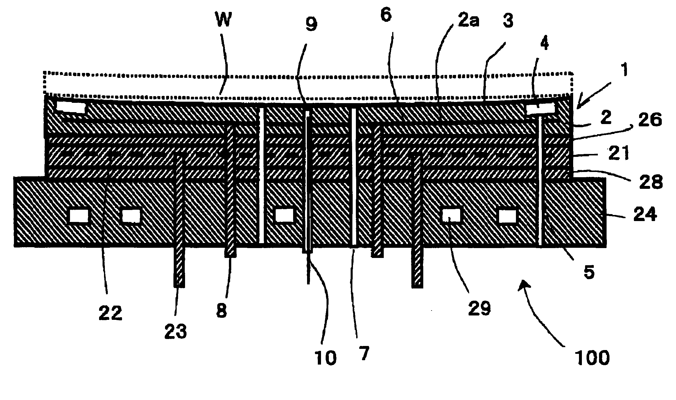
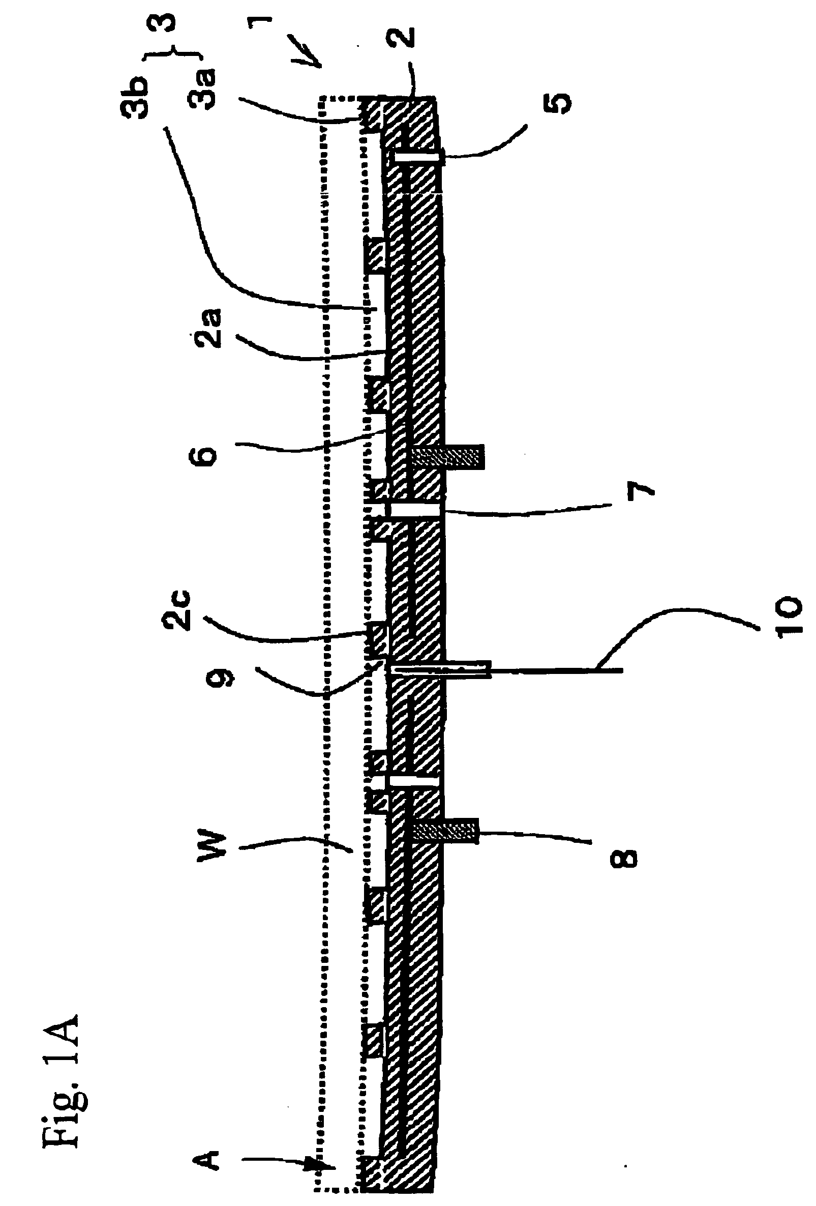
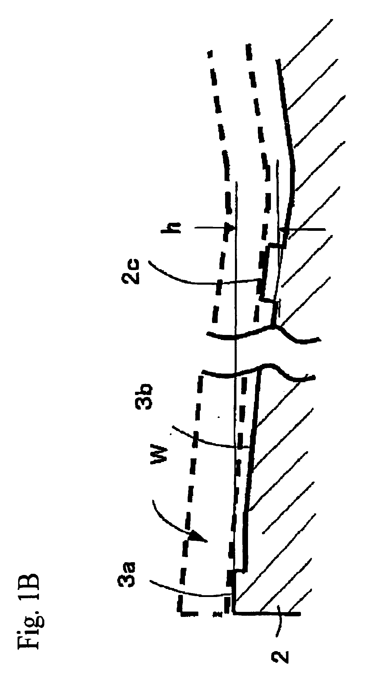
01 Electrostatic chuck electrode configuration and design
Various electrode configurations and designs are employed in electrostatic chucks to optimize wafer holding and alignment capabilities. These designs include multi-zone electrode patterns, segmented electrodes, and specialized electrode geometries that provide uniform electrostatic force distribution across the wafer surface. The electrode configuration directly impacts the chuck's ability to maintain precise wafer positioning and alignment during semiconductor processing operations.- Electrostatic chuck electrode design and configuration: Various electrode configurations and designs are employed in electrostatic chucks to improve wafer holding and alignment capabilities. These designs include multi-zone electrodes, segmented electrode patterns, and specialized electrode geometries that provide enhanced control over wafer positioning and clamping force distribution across the wafer surface.
- Wafer positioning and alignment mechanisms: Specialized mechanisms and systems are integrated with electrostatic chucks to achieve precise wafer positioning and alignment. These systems utilize various positioning elements, guides, and reference structures that work in conjunction with the electrostatic clamping force to ensure accurate wafer placement and maintain alignment during processing operations.
- Voltage control and power supply systems: Advanced voltage control systems and power supply configurations are designed to optimize the electrostatic clamping performance for wafer alignment applications. These systems provide precise control over the applied voltages, enable multi-zone voltage control, and incorporate feedback mechanisms to maintain consistent clamping forces across different wafer areas.
- Surface treatment and dielectric materials: Various surface treatments and dielectric material compositions are applied to electrostatic chuck surfaces to enhance wafer alignment performance. These treatments improve the uniformity of electrostatic forces, reduce particle generation, and provide better surface properties for consistent wafer contact and alignment repeatability.
- Temperature control and thermal management: Integrated temperature control systems are incorporated into electrostatic chucks to manage thermal effects that can impact wafer alignment accuracy. These systems include heating and cooling elements, temperature sensors, and thermal distribution features that maintain uniform temperature conditions to prevent thermal-induced wafer distortion and alignment drift.
02 Wafer alignment sensing and detection systems
Advanced sensing and detection systems are integrated with electrostatic chucks to monitor and control wafer alignment in real-time. These systems utilize various sensing technologies to detect wafer position, orientation, and any misalignment issues. The detection mechanisms enable automatic correction of wafer positioning and ensure optimal alignment throughout the processing cycle.Expand Specific Solutions03 Electrostatic force control and voltage regulation
Precise control of electrostatic forces through voltage regulation is critical for effective wafer alignment and holding. Control systems manage the application of electrical voltages to different electrode zones, allowing for fine-tuning of holding forces and alignment corrections. These systems can dynamically adjust voltages to compensate for wafer variations and maintain consistent alignment performance.Expand Specific Solutions04 Chuck surface design and wafer contact optimization
The surface design and contact interface between the electrostatic chuck and wafer are engineered to maximize alignment accuracy and minimize contamination. Surface features, texturing, and contact point optimization ensure uniform contact pressure and reduce particle generation. These design elements contribute to improved wafer flatness and alignment stability during processing operations.Expand Specific Solutions05 Integrated alignment mechanisms and positioning systems
Mechanical alignment mechanisms are integrated with electrostatic chuck systems to provide comprehensive wafer positioning capabilities. These systems combine electrostatic holding with mechanical alignment features such as guide pins, lift mechanisms, and rotational adjustment systems. The integration enables precise initial wafer placement and maintains alignment throughout the entire processing sequence.Expand Specific Solutions
Key Players in ESC and Semiconductor Equipment Industry
The electrostatic chuck optimization market is in a mature growth phase, driven by increasing demand for precision wafer handling in advanced semiconductor manufacturing. The market demonstrates significant scale with established players like Applied Materials, ASML, and Tokyo Electron leading through comprehensive equipment portfolios. Technology maturity varies considerably across the competitive landscape - while industry giants like Samsung Electronics, TSMC, and SMIC-Beijing represent advanced implementation capabilities, specialized firms such as Temnest, Beijing U-PRECISION TECH, and Kyocera focus on innovative ESC solutions and materials engineering. The sector shows strong technical differentiation, with companies like Niterra and Saint-Gobain Ceramics advancing ceramic technologies, while newer entrants like Skyverse Technology contribute measurement and inspection capabilities. This competitive environment reflects a technologically sophisticated market where established semiconductor equipment manufacturers compete alongside specialized component suppliers and emerging technology developers, indicating robust innovation potential in electrostatic chuck optimization for enhanced wafer alignment precision.
Applied Materials, Inc.
Technical Solution: Applied Materials has developed advanced electrostatic chuck (ESC) systems featuring multi-zone temperature control and enhanced clamping force distribution for precise wafer alignment. Their ESC technology incorporates proprietary ceramic materials with optimized dielectric properties and embedded electrode patterns that provide uniform electrostatic force across the wafer surface. The company's ESC solutions include real-time feedback control systems that monitor wafer position and automatically adjust clamping forces to maintain optimal alignment during processing. Their latest generation ESCs feature improved thermal management with integrated cooling channels and advanced surface treatments to minimize particle generation and enhance wafer release characteristics.
Strengths: Industry-leading technology with comprehensive process integration capabilities and extensive R&D resources. Weaknesses: High cost and complex system requirements may limit adoption in cost-sensitive applications.
Kyocera Corp.
Technical Solution: Kyocera has developed advanced ceramic-based electrostatic chuck systems utilizing their proprietary fine ceramic technology with enhanced dielectric properties and thermal conductivity for superior wafer alignment performance. Their ESC solutions feature multi-layered ceramic substrates with precisely controlled porosity and embedded electrode patterns that provide uniform electrostatic force distribution across the entire wafer surface. The company's chuck technology incorporates advanced surface finishing techniques and specialized coatings that minimize particle generation while maintaining excellent wafer release characteristics. Kyocera's ESCs are designed with integrated thermal management systems and real-time monitoring capabilities to ensure consistent performance across varying process conditions and extended operational cycles.
Strengths: Superior ceramic material expertise with excellent thermal properties and proven durability in harsh processing environments. Weaknesses: Limited system integration capabilities compared to full equipment manufacturers and higher material costs.
Core Patents in ESC Design for Precision Alignment
Methods for electrostatic chuck ceramic surfacing
PatentWO2023146808A1
Innovation
- The method involves planarizing the upper ceramic surface of ESCs using techniques like bead blasting, polishing, lapping, or chemical mechanical planarization to achieve specific surface morphology parameters such as arithmetical mean height (Sa) of less than 0.1 microns, developed interfacial area ratio (Sdr) of less than 2.5 percent, and maximum peak to valley (Sz) of less than 10 microns, ensuring stable and reliable chucking performance.


Electrostatic chuck and wafer holding member and wafer treatment method
PatentActiveUS20060209490A1
Innovation
- An electrostatic chuck with a plate-shaped ceramic body featuring a circular projected part in the circumferential rim and a circular recessed part, where the arithmetic mean deviation ratio is maintained at 0.2 or lower, and a smooth concave face for uniform gas packing, combined with a heat radiating sheet and cooling member for improved heat transfer and temperature control.

Semiconductor Manufacturing Standards and ESC Requirements
The semiconductor manufacturing industry operates under stringent standards that directly influence electrostatic chuck design and performance requirements. International standards such as SEMI E88 for wafer handling equipment and SEMI E15 for safety guidelines establish fundamental parameters that ESC systems must meet. These standards define critical specifications including wafer flatness tolerances, typically within 0.5 micrometers across the wafer surface, and contamination control requirements that mandate particle-free environments during wafer processing.
Temperature uniformity represents a cornerstone requirement in semiconductor manufacturing standards, with ESC systems required to maintain thermal variations below ±2°C across the entire wafer surface. This specification becomes increasingly challenging as wafer sizes expand to 300mm and beyond, necessitating sophisticated chuck designs with multiple heating zones and advanced temperature control algorithms. The standards also mandate rapid thermal response capabilities, requiring ESC systems to achieve target temperatures within specified timeframes while maintaining uniform heat distribution.
Electrostatic force uniformity standards demand that ESC systems generate consistent clamping forces across the wafer surface, typically requiring force variations to remain within ±5% of the nominal value. This requirement directly impacts electrode design patterns and voltage distribution systems within the chuck. Manufacturing standards also specify minimum and maximum clamping forces to ensure adequate wafer retention without inducing mechanical stress that could cause wafer warpage or breakage.
Contamination control requirements under cleanroom standards significantly influence ESC material selection and surface treatments. The chucks must demonstrate compatibility with aggressive cleaning chemicals while maintaining electrostatic properties over extended operational cycles. Standards mandate that ESC surfaces exhibit minimal particle generation and resist chemical degradation when exposed to plasma environments and cleaning solvents commonly used in semiconductor fabrication.
Reliability and lifetime requirements established by industry standards typically specify minimum operational cycles exceeding 100,000 wafer processing events without performance degradation. These standards drive material selection toward ceramics and specialized coatings that can withstand repeated thermal cycling, chemical exposure, and mechanical stress while maintaining precise dimensional stability and electrical properties essential for consistent wafer alignment performance.
ESC Material Science and Surface Engineering Advances
The advancement of electrostatic chuck (ESC) material science has become increasingly critical for achieving precise wafer alignment in semiconductor manufacturing. Modern ESC systems rely on sophisticated material compositions that balance electrical conductivity, thermal stability, and mechanical durability. Advanced ceramic materials, particularly aluminum nitride (AlN) and silicon carbide (SiC) composites, have emerged as preferred substrates due to their superior thermal conductivity and low coefficient of thermal expansion, which directly impacts wafer positioning accuracy.
Surface engineering innovations have revolutionized ESC performance through the development of multi-layered dielectric coatings. These engineered surfaces incorporate nanostructured materials that enhance electrostatic force distribution while minimizing surface roughness variations. Recent breakthroughs in atomic layer deposition (ALD) techniques enable the creation of ultra-thin, uniform dielectric layers with precise thickness control at the nanometer scale, significantly improving wafer clamping uniformity and alignment precision.
The integration of smart materials into ESC design represents a paradigm shift in wafer handling technology. Shape memory alloys and piezoelectric materials are being incorporated into ESC structures to provide active surface adjustment capabilities. These materials can compensate for thermal expansion mismatches and provide real-time surface flatness corrections, enhancing wafer alignment stability during processing cycles.
Plasma-resistant coatings have evolved to address the challenges of aggressive semiconductor processing environments. Advanced fluoropolymer composites and diamond-like carbon (DLC) coatings demonstrate exceptional resistance to plasma etching while maintaining consistent surface properties. These materials prevent particle generation and surface degradation that could compromise wafer alignment accuracy over extended operational periods.
Surface texturing technologies have advanced to create micro-engineered topographies that optimize gas flow patterns beneath wafers. Controlled surface roughness and micro-channel designs facilitate uniform gas distribution for backside cooling while maintaining consistent electrostatic forces across the wafer surface. These engineered surfaces contribute to improved thermal management and enhanced wafer flatness control during high-temperature processing operations.
Unlock deeper insights with PatSnap Eureka Quick Research — get a full tech report to explore trends and direct your research. Try now!
Generate Your Research Report Instantly with AI Agent
Supercharge your innovation with PatSnap Eureka AI Agent Platform!