Multi Chip Module vs Heterogeneous ICs: Processing Challenges
MAR 12, 20269 MIN READ
Generate Your Research Report Instantly with AI Agent
Patsnap Eureka helps you evaluate technical feasibility & market potential.
MCM vs Heterogeneous IC Processing Background and Objectives
The semiconductor industry has witnessed a fundamental shift in packaging and integration strategies over the past two decades, driven by the relentless pursuit of higher performance, reduced power consumption, and enhanced functionality. This evolution has led to two distinct yet complementary approaches: Multi Chip Modules (MCMs) and Heterogeneous Integrated Circuits (ICs), each presenting unique processing challenges that demand innovative manufacturing solutions.
Multi Chip Module technology emerged as a response to the limitations of traditional single-chip solutions, enabling the integration of multiple discrete semiconductor dies within a single package. This approach allows for the combination of different process technologies, materials, and functionalities that would be impossible or economically unfeasible to implement on a single silicon substrate. MCMs have found particular success in high-performance computing, telecommunications, and aerospace applications where system-level optimization takes precedence over individual component performance.
Heterogeneous IC integration represents a more recent paradigm shift, focusing on the monolithic integration of diverse functional blocks using advanced process technologies such as 3D stacking, through-silicon vias (TSVs), and advanced packaging techniques. This approach aims to achieve higher integration density while maintaining or improving performance metrics compared to traditional homogeneous designs.
The primary objective of comparing these two integration strategies lies in understanding their respective processing challenges and identifying optimal application scenarios. Key technical goals include evaluating thermal management solutions, analyzing interconnect density and signal integrity requirements, assessing manufacturing yield implications, and determining cost-effectiveness across different market segments.
Processing challenges in MCM technology primarily revolve around substrate design complexity, multi-die assembly precision, and thermal interface management. The heterogeneous nature of components requires sophisticated design rules to accommodate different coefficient of thermal expansion values, varying power densities, and diverse electrical requirements within a single package.
Heterogeneous IC processing faces distinct challenges related to process compatibility, yield optimization across different functional blocks, and advanced lithography requirements for high-density interconnects. The integration of analog, digital, and RF components on a single substrate demands careful consideration of process interactions, contamination control, and performance isolation techniques.
Understanding these processing challenges is crucial for developing next-generation semiconductor solutions that can meet the increasing demands for higher performance, lower power consumption, and enhanced functionality in emerging applications such as artificial intelligence, 5G communications, and autonomous systems.
Market Demand for Advanced Multi-Chip Integration Solutions
The semiconductor industry is experiencing unprecedented demand for advanced multi-chip integration solutions, driven by the convergence of artificial intelligence, high-performance computing, and edge computing applications. This surge reflects the industry's response to the physical limitations of traditional monolithic chip scaling and the growing need for specialized processing capabilities within single packages.
Data centers and cloud computing infrastructure represent the largest market segment for advanced integration solutions. Hyperscale data center operators are increasingly adopting multi-chip modules and heterogeneous integrated circuits to optimize performance per watt while managing thermal constraints. The demand stems from workloads requiring diverse processing elements, including CPUs, GPUs, memory controllers, and specialized accelerators operating in close proximity.
The automotive sector is emerging as a significant growth driver, particularly with the advancement of autonomous driving technologies. Modern vehicles require sophisticated computing platforms that integrate sensor processing, real-time decision-making, and communication capabilities. Multi-chip integration enables automotive manufacturers to consolidate multiple functions while meeting stringent reliability and safety requirements.
Mobile and edge computing applications are creating substantial demand for heterogeneous integration solutions that combine processing power with energy efficiency. The proliferation of Internet of Things devices and edge AI applications requires compact, power-efficient solutions that can handle diverse computational tasks without compromising performance or battery life.
Telecommunications infrastructure modernization, particularly the deployment of 5G networks, is generating significant market pull for advanced integration technologies. Network equipment manufacturers require solutions that can handle high-frequency signal processing, baseband processing, and network management functions within space-constrained environments.
The gaming and graphics processing market continues to drive innovation in multi-chip integration, with demands for higher resolution displays, real-time ray tracing, and immersive virtual reality experiences. These applications require tight integration between graphics processors, memory systems, and specialized compute units.
Enterprise computing and high-performance computing segments are increasingly adopting heterogeneous integration to address complex computational challenges in scientific research, financial modeling, and machine learning applications. The market demand reflects the need for solutions that can efficiently handle both parallel processing and specialized computational tasks within unified architectures.
Current Processing Challenges in MCM and Heterogeneous IC Manufacturing
Multi Chip Module and heterogeneous IC manufacturing face significant processing challenges that stem from the fundamental differences in their architectural approaches and fabrication requirements. These challenges have become increasingly complex as the semiconductor industry pushes toward higher integration densities and performance targets while managing cost constraints.
Thermal management represents one of the most critical challenges in both MCM and heterogeneous IC manufacturing. In MCM configurations, multiple discrete chips generate concentrated heat loads that must be efficiently dissipated through sophisticated thermal interface materials and heat spreading solutions. The challenge intensifies when chips with different power densities are integrated within the same package, creating thermal gradients that can affect performance and reliability.
Interconnect complexity poses another major hurdle, particularly in achieving reliable electrical connections between disparate chip technologies. MCM assemblies require precise wire bonding or flip-chip connections across multiple die, each potentially operating at different voltage levels and signal frequencies. Heterogeneous ICs face similar challenges in creating seamless interconnections between different process nodes or material systems integrated on the same substrate.
Manufacturing yield optimization becomes exponentially more difficult when multiple chips or heterogeneous elements are combined. In MCM production, the overall yield is the product of individual chip yields, meaning that a single defective component can render the entire module unusable. This multiplicative effect significantly impacts cost-effectiveness and requires sophisticated testing strategies to identify defective components before final assembly.
Process integration challenges arise from the need to accommodate different manufacturing requirements within a single production flow. Heterogeneous ICs often require multiple lithography steps, varied etching processes, and different material deposition techniques to accommodate diverse device types. This complexity increases manufacturing cycle times and requires specialized equipment capable of handling multiple process variations.
Quality control and testing present unique difficulties due to the increased complexity of multi-chip and heterogeneous systems. Traditional testing methodologies may not adequately address the interactions between different chip types or the performance variations that can occur at the interfaces between heterogeneous elements. Advanced testing protocols must account for system-level performance while maintaining the ability to isolate individual component failures.
Supply chain coordination becomes more challenging when multiple chip types from different suppliers must be integrated into a single product. This requires careful inventory management, quality alignment across suppliers, and synchronized production schedules to minimize assembly delays and maintain consistent product quality standards.
Existing Processing Solutions for Multi-Chip Integration
01 Thermal management and heat dissipation in multi-chip modules
Multi-chip modules face significant thermal challenges due to the high power density and heat generation from multiple integrated circuits in close proximity. Effective thermal management solutions include advanced heat sink designs, thermal interface materials, and cooling structures that facilitate heat dissipation. These solutions address the challenge of maintaining optimal operating temperatures while preventing thermal crosstalk between adjacent chips in heterogeneous integration scenarios.- Thermal management and heat dissipation in multi-chip modules: Multi-chip modules face significant thermal challenges due to the high power density and heat generation from multiple integrated circuits in close proximity. Effective thermal management solutions include advanced heat sink designs, thermal interface materials, and cooling structures that facilitate heat dissipation. These solutions address the challenge of maintaining optimal operating temperatures while preventing thermal crosstalk between adjacent chips in heterogeneous integration scenarios.
- Interconnection and bonding techniques for heterogeneous integration: Heterogeneous ICs require advanced interconnection methods to integrate chips with different materials, processes, and functionalities. Wire bonding, flip-chip bonding, through-silicon vias, and micro-bump technologies enable electrical connections between diverse chip types. These techniques must address challenges such as coefficient of thermal expansion mismatch, mechanical stress, and reliability concerns while maintaining signal integrity across different semiconductor technologies.
- Testing and quality control methodologies for multi-chip systems: Testing multi-chip modules presents unique challenges as individual chips must be verified before and after assembly, requiring specialized test structures and methodologies. Built-in self-test circuits, boundary scan techniques, and known-good-die screening processes help ensure functionality and reliability. The complexity increases with heterogeneous integration where different chip types require distinct test protocols and failure analysis approaches.
- Substrate and packaging design for heterogeneous chip integration: Advanced substrate technologies and packaging architectures are essential for accommodating multiple chips with varying sizes, thicknesses, and I/O requirements. Multi-layer substrates with fine-pitch routing, embedded passive components, and redistribution layers enable compact integration. Package designs must address challenges including signal routing complexity, power distribution, electromagnetic interference, and mechanical stability for chips manufactured using different process nodes.
- Manufacturing process integration and yield optimization: Processing heterogeneous ICs in multi-chip modules requires careful integration of different manufacturing processes, materials, and assembly sequences. Challenges include alignment accuracy, contamination control, process compatibility, and yield management across diverse chip types. Advanced manufacturing techniques such as wafer-level processing, die placement automation, and adaptive process control help optimize production efficiency and reduce defects in complex multi-chip assemblies.
02 Interconnection and bonding techniques for heterogeneous integration
Heterogeneous ICs require advanced interconnection methods to integrate chips with different materials, processes, and functionalities. Wire bonding, flip-chip bonding, through-silicon vias, and micro-bump technologies enable electrical connections between diverse chip types. These techniques must address challenges such as coefficient of thermal expansion mismatch, mechanical stress, and reliability concerns while maintaining signal integrity across different semiconductor technologies.Expand Specific Solutions03 Testing and quality control methodologies for multi-chip systems
Testing multi-chip modules presents unique challenges due to the complexity of verifying multiple integrated circuits simultaneously. Advanced testing strategies include built-in self-test capabilities, boundary scan techniques, and specialized test structures that enable comprehensive functional and parametric testing. Quality control methods must address the difficulty of isolating defects in individual chips within the module and ensuring overall system reliability.Expand Specific Solutions04 Substrate design and packaging solutions for heterogeneous integration
Multi-chip modules require sophisticated substrate designs that accommodate different chip sizes, I/O configurations, and power requirements. Advanced packaging solutions include multi-layer substrates with embedded passive components, redistribution layers, and specialized materials that provide mechanical support and electrical routing. These designs must address challenges related to signal routing density, power distribution, electromagnetic interference, and overall package miniaturization.Expand Specific Solutions05 Manufacturing process integration and yield optimization
Processing heterogeneous ICs in multi-chip modules involves integrating diverse manufacturing processes and materials, which creates yield and reliability challenges. Process integration techniques address issues such as handling chips from different fabrication technologies, managing process compatibility, and optimizing assembly sequences. Yield optimization strategies include known-good-die testing, adaptive process control, and defect management systems that improve overall manufacturing efficiency and product quality.Expand Specific Solutions
Key Players in MCM and Heterogeneous IC Industry
The multi-chip module versus heterogeneous IC processing challenge represents a rapidly evolving competitive landscape driven by increasing demand for specialized computing architectures. The industry is transitioning from mature single-chip solutions to advanced heterogeneous integration approaches, with market growth fueled by AI, 5G, and edge computing applications. Technology maturity varies significantly across players, with established leaders like Intel, TSMC, and Samsung demonstrating advanced packaging capabilities, while companies such as AMD, Qualcomm, and Huawei are aggressively pursuing chiplet and heterogeneous designs. Foundries including SMIC are expanding advanced packaging services, and specialized firms like Xilinx (now part of AMD) and Altera are pioneering programmable heterogeneous solutions. The competitive dynamics reflect a shift toward collaborative ecosystems where traditional boundaries between chip designers, foundries, and system integrators are blurring to address complex processing challenges.
Intel Corp.
Technical Solution: Intel has developed advanced Multi-Chip Module (MCM) architectures including their Ponte Vecchio GPU which integrates over 40 tiles using advanced packaging technologies like EMIB (Embedded Multi-die Interconnect Bridge) and Foveros 3D stacking. Their approach addresses processing challenges through heterogeneous integration of compute, memory, and I/O tiles with optimized interconnect bandwidth exceeding 4TB/s between tiles. Intel's MCM strategy focuses on chiplet-based designs that enable mixing different process nodes and IP blocks while maintaining coherent memory access and reducing thermal hotspots through distributed processing across multiple dies.
Strengths: Advanced packaging technologies, high interconnect bandwidth, proven chiplet architecture. Weaknesses: Complex thermal management, higher power consumption in some configurations.
QUALCOMM, Inc.
Technical Solution: Qualcomm leverages heterogeneous IC design in their Snapdragon SoCs, integrating multiple specialized processing units including CPU clusters, GPU, DSP, NPU, and modem on a single die. Their approach addresses processing challenges through asymmetric multiprocessing with big.LITTLE CPU architecture and dedicated accelerators for AI workloads achieving up to 35 TOPS performance. For advanced applications, Qualcomm explores MCM approaches in their automotive and edge AI platforms, utilizing advanced packaging to combine different silicon technologies while maintaining power efficiency below 5W for mobile applications.
Strengths: Integrated heterogeneous design expertise, power efficiency optimization, strong mobile market presence. Weaknesses: Limited high-performance computing focus, primarily single-die integration.
Core Processing Innovations in MCM and Heterogeneous IC
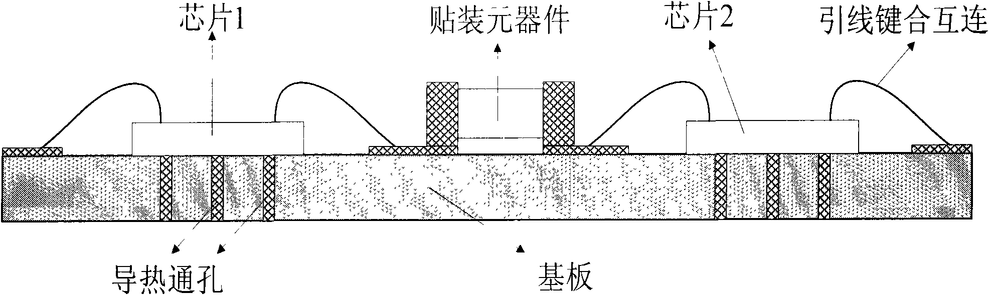
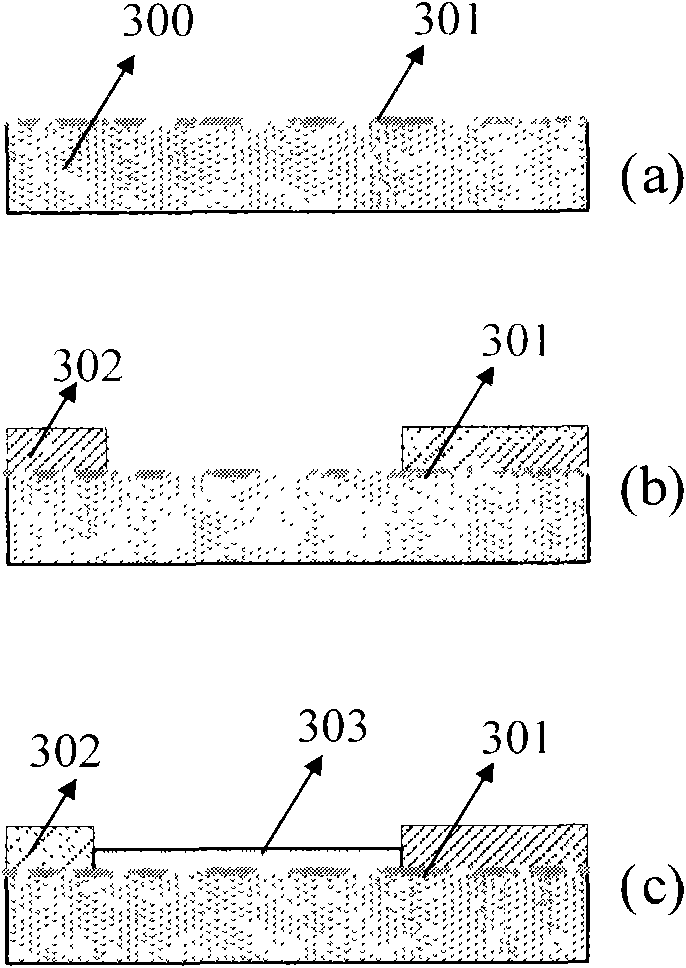
Multilayer interconnection structure of wafer level package, manufacturing method and application
PatentInactiveCN101656249A
Innovation
- Organic polymers such as benzocyclobutene (BCB) polyimide or SU8 are used as the dielectric layer, combined with mechanical polishing technology, to form a multi-layer interconnection structure with alternating metal layers and dielectric layers, reducing the thickness of the dielectric layer and increasing packaging density. , using a combination of electroplating and mechanical polishing to achieve vertical interconnections and embedded passive components.

Multi-chip modules
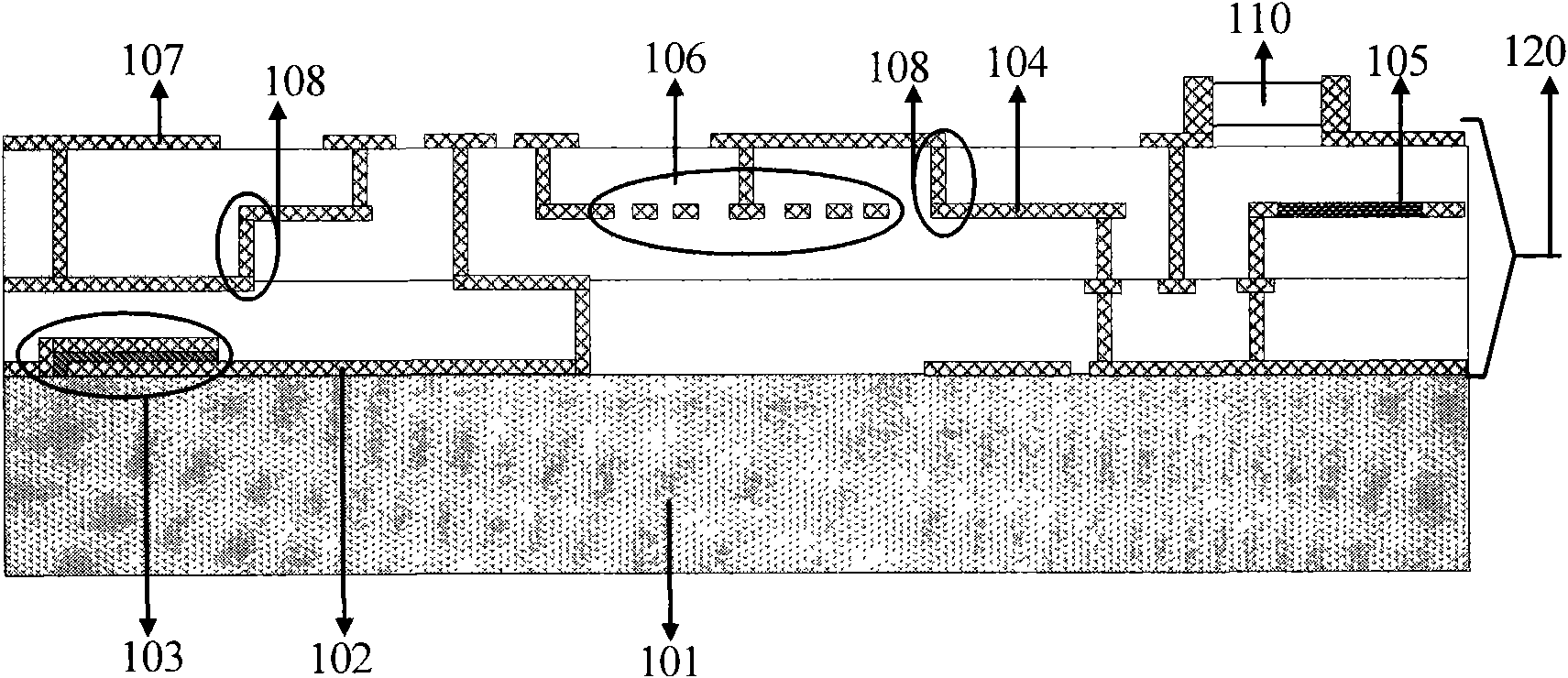
PatentActiveUS20200235086A1
Innovation
- The method involves forming semiconductor components with different pitch dimensions for connections and interconnecting them using solder bump and pad connections, eliminating the need for TSVs or substrate wires, allowing for a stacked multi-chip module configuration.


Thermal Management Strategies for Multi-Chip Systems
Thermal management represents one of the most critical challenges in multi-chip module (MCM) and heterogeneous IC systems, where multiple processing units generate concentrated heat loads within confined spaces. The complexity arises from the heterogeneous nature of these systems, where different chip types exhibit varying thermal characteristics, power densities, and temperature sensitivities.
Advanced thermal interface materials (TIMs) have emerged as fundamental components for effective heat dissipation in multi-chip architectures. These materials, including phase-change materials, liquid metals, and carbon nanotube composites, facilitate efficient heat transfer between chips and cooling systems. The selection of appropriate TIMs depends on the specific thermal conductivity requirements, mechanical compliance, and long-term reliability considerations of the integrated system.
Microchannel cooling solutions represent a sophisticated approach for managing hotspots in densely packed multi-chip configurations. These systems utilize precisely engineered microfluidic channels that enable targeted cooling of high-power density regions. The implementation requires careful consideration of flow distribution, pressure drop optimization, and integration with existing packaging technologies to ensure uniform temperature distribution across heterogeneous chip arrays.
Three-dimensional thermal modeling and simulation tools have become indispensable for predicting thermal behavior in complex multi-chip systems. These computational approaches enable engineers to optimize chip placement, thermal pathway design, and cooling system configuration before physical implementation. Advanced modeling techniques incorporate transient thermal analysis, considering dynamic power variations and thermal coupling effects between adjacent chips.
Innovative packaging architectures, such as through-silicon vias (TSVs) and embedded cooling structures, provide enhanced thermal pathways for heat extraction. These solutions enable vertical heat conduction and distributed thermal management, particularly beneficial for 3D-stacked multi-chip modules where conventional lateral cooling approaches prove insufficient.
Active thermal management strategies, including on-chip temperature sensors and dynamic thermal throttling, offer real-time thermal control capabilities. These systems continuously monitor temperature distributions and adjust operating parameters to prevent thermal runaway conditions while maintaining optimal performance across all integrated components in heterogeneous multi-chip systems.
Yield Optimization in Complex Multi-Chip Processing
Yield optimization in complex multi-chip processing represents one of the most critical challenges in modern semiconductor manufacturing, particularly when comparing Multi Chip Module (MCM) and heterogeneous IC approaches. The fundamental challenge lies in the multiplicative nature of yield degradation, where the overall system yield equals the product of individual component yields. In MCM architectures, this translates to potentially severe yield penalties when multiple discrete chips are integrated, as each additional component introduces its own failure probability.
The statistical nature of yield optimization becomes particularly complex in multi-chip environments due to the diverse failure modes across different chip types. Memory chips, logic processors, and analog components each exhibit distinct defect patterns and sensitivity profiles. Advanced yield modeling techniques now incorporate machine learning algorithms to predict and mitigate these multi-dimensional failure scenarios, enabling more sophisticated binning strategies that can salvage partially functional multi-chip assemblies.
Process-induced yield challenges in complex multi-chip processing stem from the inherent variability in manufacturing parameters across different chip types. Thermal cycling during assembly processes can introduce mechanical stress variations, while the diverse material properties of different chip substrates create non-uniform expansion coefficients. These factors contribute to interconnect reliability issues and can significantly impact long-term yield performance.
Advanced packaging technologies have introduced novel yield optimization strategies specifically designed for multi-chip environments. Through-silicon via (TSV) technology enables three-dimensional integration while maintaining acceptable yield levels through redundancy schemes and adaptive routing capabilities. Similarly, advanced underfill materials and thermal interface solutions help mitigate stress-related failures that traditionally plagued multi-chip assemblies.
Statistical process control in multi-chip manufacturing requires sophisticated monitoring systems that can track yield performance across multiple chip types simultaneously. Real-time feedback mechanisms enable dynamic adjustment of assembly parameters, while predictive analytics help identify potential yield excursions before they impact production volumes. These systems must account for the complex interdependencies between different chip types and their cumulative impact on overall system functionality.
The economic implications of yield optimization in multi-chip processing extend beyond simple manufacturing costs. Known good die (KGD) testing strategies become crucial for maintaining acceptable overall yields, as incorporating a single defective chip can render an entire multi-chip module non-functional. Advanced testing methodologies, including built-in self-test (BIST) capabilities and boundary scan techniques, enable more effective screening of individual components before assembly.
Unlock deeper insights with Patsnap Eureka Quick Research — get a full tech report to explore trends and direct your research. Try now!
Generate Your Research Report Instantly with AI Agent
Supercharge your innovation with Patsnap Eureka AI Agent Platform!