

Optimize NanoStructures in Thermoelectric Generators
MAR 9, 20269 MIN READ
Generate Your Research Report Instantly with AI Agent
PatSnap Eureka helps you evaluate technical feasibility & market potential.
Nanostructure Thermoelectric Background and Objectives
Thermoelectric technology has emerged as a critical solution for sustainable energy conversion, enabling direct transformation between thermal and electrical energy without moving parts or harmful emissions. The fundamental principle relies on the Seebeck effect, where temperature gradients across semiconductor materials generate electrical voltage, making it particularly valuable for waste heat recovery and remote power generation applications.
The evolution of thermoelectric materials has progressed through distinct phases, beginning with bulk semiconductor alloys in the 1950s and advancing toward sophisticated nanostructured architectures. Early developments focused on bismuth telluride and lead telluride compounds, achieving modest efficiency levels suitable for niche applications like space missions and specialized cooling systems.
Contemporary research has shifted toward nanostructure optimization as the primary pathway for enhancing thermoelectric performance. The dimensionality reduction from bulk to nanoscale structures fundamentally alters phonon transport mechanisms while preserving electronic properties, creating unprecedented opportunities for efficiency improvements. Quantum confinement effects in low-dimensional structures enable selective manipulation of charge carrier distributions and energy band structures.
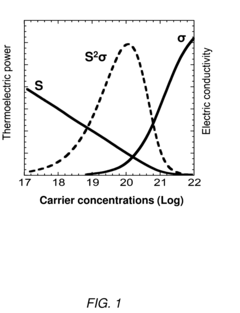
The core challenge lies in simultaneously optimizing the thermoelectric figure of merit ZT, which requires maximizing electrical conductivity and Seebeck coefficient while minimizing thermal conductivity. Traditional bulk materials face inherent limitations due to interdependent transport properties, where improvements in one parameter often compromise others. Nanostructuring offers decoupled control over these competing factors through engineered interfaces and quantum effects.
Current objectives focus on achieving ZT values exceeding 2.0 for commercial viability, compared to typical bulk material values around 1.0. This ambitious target necessitates revolutionary approaches in nanostructure design, including superlattices, quantum dots, nanowires, and hierarchical architectures. The integration of advanced computational modeling with experimental synthesis techniques has become essential for systematic optimization.
The strategic importance extends beyond energy conversion efficiency to encompass scalable manufacturing processes and material stability under operational conditions. Successful nanostructure optimization must address thermal cycling durability, interface stability, and cost-effective production methods to enable widespread commercial deployment across automotive, industrial, and consumer electronics sectors.
The evolution of thermoelectric materials has progressed through distinct phases, beginning with bulk semiconductor alloys in the 1950s and advancing toward sophisticated nanostructured architectures. Early developments focused on bismuth telluride and lead telluride compounds, achieving modest efficiency levels suitable for niche applications like space missions and specialized cooling systems.
Contemporary research has shifted toward nanostructure optimization as the primary pathway for enhancing thermoelectric performance. The dimensionality reduction from bulk to nanoscale structures fundamentally alters phonon transport mechanisms while preserving electronic properties, creating unprecedented opportunities for efficiency improvements. Quantum confinement effects in low-dimensional structures enable selective manipulation of charge carrier distributions and energy band structures.
The core challenge lies in simultaneously optimizing the thermoelectric figure of merit ZT, which requires maximizing electrical conductivity and Seebeck coefficient while minimizing thermal conductivity. Traditional bulk materials face inherent limitations due to interdependent transport properties, where improvements in one parameter often compromise others. Nanostructuring offers decoupled control over these competing factors through engineered interfaces and quantum effects.
Current objectives focus on achieving ZT values exceeding 2.0 for commercial viability, compared to typical bulk material values around 1.0. This ambitious target necessitates revolutionary approaches in nanostructure design, including superlattices, quantum dots, nanowires, and hierarchical architectures. The integration of advanced computational modeling with experimental synthesis techniques has become essential for systematic optimization.
The strategic importance extends beyond energy conversion efficiency to encompass scalable manufacturing processes and material stability under operational conditions. Successful nanostructure optimization must address thermal cycling durability, interface stability, and cost-effective production methods to enable widespread commercial deployment across automotive, industrial, and consumer electronics sectors.
Market Demand for Advanced Thermoelectric Generators
The global thermoelectric generator market is experiencing unprecedented growth driven by increasing demand for sustainable energy solutions and waste heat recovery applications. Industrial sectors are recognizing the potential of thermoelectric technology to convert waste heat into usable electricity, creating substantial market opportunities for advanced thermoelectric systems with optimized nanostructures.
Automotive manufacturers represent a significant demand driver, seeking thermoelectric generators to improve fuel efficiency by recovering waste heat from exhaust systems. The push toward stricter emission regulations and fuel economy standards has intensified interest in thermoelectric solutions that can enhance overall vehicle efficiency. Electric vehicle manufacturers are also exploring thermoelectric applications for battery thermal management and range extension.
The aerospace and defense sectors demonstrate strong demand for compact, reliable thermoelectric generators capable of operating in extreme environments. Space missions require power generation systems that can function without moving parts, making advanced thermoelectric devices with optimized nanostructures particularly attractive for satellite applications and deep space exploration missions.
Industrial waste heat recovery presents the largest market opportunity, with manufacturing facilities, power plants, and chemical processing operations generating substantial amounts of recoverable thermal energy. Steel production, cement manufacturing, and glass production industries are actively seeking thermoelectric solutions to improve energy efficiency and reduce operational costs.
Consumer electronics applications are emerging as a growing market segment, with wearable devices and IoT sensors requiring miniaturized power generation solutions. The demand for self-powered sensors and remote monitoring systems is driving interest in thermoelectric generators that can harvest ambient thermal energy.
The renewable energy sector is increasingly incorporating thermoelectric generators as complementary power generation systems, particularly in hybrid solar-thermal applications and geothermal energy harvesting. This integration approach maximizes energy conversion efficiency across multiple thermal gradients.
Market demand is particularly strong for thermoelectric generators offering improved efficiency, reduced manufacturing costs, and enhanced durability. End users prioritize systems that can operate reliably across wide temperature ranges while maintaining consistent power output, driving the need for advanced nanostructure optimization technologies.
Current Nanostructure TEG Status and Challenges
Nanostructured thermoelectric generators have achieved significant progress in recent years, with ZT values reaching 2.0-2.5 in laboratory conditions for materials like PbTe, Bi2Te3, and SnSe systems. Advanced nanostructuring techniques including quantum dots, nanowires, superlattices, and nanocomposites have demonstrated enhanced phonon scattering while preserving electrical conductivity. Commercial applications primarily focus on waste heat recovery in automotive exhaust systems and industrial processes, though efficiency remains limited to 5-8% in practical implementations.
Current fabrication methods encompass bottom-up approaches such as chemical vapor deposition, molecular beam epitaxy, and solution-based synthesis, alongside top-down techniques including electron beam lithography and reactive ion etching. These methods enable precise control over nanostructure dimensions, composition gradients, and interface engineering. However, scalability and cost-effectiveness remain significant barriers for widespread commercial adoption.
The primary technical challenges center on the fundamental trade-off between electrical and thermal transport properties. While nanostructuring effectively reduces lattice thermal conductivity through enhanced phonon-boundary scattering, it often simultaneously degrades electrical conductivity and Seebeck coefficient due to increased carrier scattering at interfaces and grain boundaries. Achieving optimal balance requires precise control over carrier concentration, mobility, and phonon mean free path.
Manufacturing scalability presents another critical obstacle. Laboratory-scale synthesis methods often cannot be directly translated to industrial production volumes while maintaining nanostructure quality and uniformity. Process reproducibility, yield optimization, and quality control become increasingly complex as feature sizes approach atomic scales. Additionally, nanostructured materials frequently exhibit thermal and mechanical instability under operating conditions, leading to performance degradation over time.
Interface engineering remains poorly understood, particularly regarding charge and phonon transport across heterointerfaces in nanocomposite systems. The relationship between nanostructure morphology, defect density, and transport properties requires further investigation to enable rational design approaches rather than empirical optimization.
Cost considerations significantly impact commercial viability, as current nanostructuring processes often require expensive equipment, high-purity materials, and controlled environments. The economic feasibility of nanostructured TEGs depends on achieving substantial performance improvements that justify increased manufacturing complexity and material costs compared to conventional bulk thermoelectric devices.
Existing Nanostructure Optimization Solutions
01 Nanostructured thermoelectric materials with enhanced ZT values
Nanostructured thermoelectric materials exhibit improved figure of merit (ZT) through quantum confinement effects and reduced thermal conductivity. These materials utilize nanoscale features such as nanowires, nanodots, or nanocomposites to enhance the power factor while maintaining low thermal conductivity. The nanostructures create phonon scattering centers that reduce lattice thermal conductivity without significantly affecting electrical conductivity, thereby improving overall thermoelectric performance.- Nanostructured thermoelectric materials with enhanced ZT values: Nanostructured thermoelectric materials exhibit improved figure of merit (ZT) through quantum confinement effects and reduced thermal conductivity. These materials utilize nanoscale features such as nanowires, nanodots, or nanocomposites to enhance the power factor while maintaining low thermal conductivity. The nanostructures create phonon scattering centers that reduce lattice thermal conductivity without significantly affecting electrical conductivity, thereby improving overall thermoelectric performance.
- Superlattice and multilayer nanostructures for thermoelectric applications: Superlattice structures consisting of alternating thin layers of different thermoelectric materials at the nanoscale provide enhanced thermoelectric properties. These multilayer configurations exploit interface effects and quantum well structures to improve the Seebeck coefficient and reduce thermal conductivity. The periodic arrangement of layers creates energy filtering effects that preferentially transport high-energy carriers while blocking phonon transport.
- Nanoparticle-embedded bulk thermoelectric materials: Bulk thermoelectric materials embedded with nanoparticles demonstrate improved performance through enhanced phonon scattering at nanoparticle-matrix interfaces. This approach combines the advantages of nanostructuring with the mechanical stability and ease of processing of bulk materials. The dispersed nanoparticles act as scattering centers for phonons while minimally affecting electron transport, leading to reduced thermal conductivity and improved ZT values.
- Nanowire and nanorod arrays in thermoelectric devices: One-dimensional nanostructures such as nanowires and nanorods arranged in arrays offer unique advantages for thermoelectric generators. These structures provide high surface-to-volume ratios and enable efficient charge carrier transport along the wire axis while promoting phonon scattering at boundaries. The array configuration allows for scalable device fabrication and can be integrated into flexible or miniaturized thermoelectric generators.
- Nanostructured electrode interfaces and contact optimization: Optimized nanostructured interfaces between thermoelectric materials and electrodes enhance device performance by reducing contact resistance and improving thermal management. These interfaces may incorporate nanoscale barrier layers, graded compositions, or textured surfaces to facilitate efficient charge transfer while minimizing thermal losses. Proper interface engineering at the nanoscale is critical for maximizing the overall efficiency of thermoelectric generators.
02 Superlattice and multilayer nanostructures for thermoelectric applications
Superlattice structures consisting of alternating thin layers of different thermoelectric materials at the nanoscale provide enhanced thermoelectric properties. These multilayer configurations exploit interface effects and quantum well structures to improve the Seebeck coefficient and reduce thermal conductivity. The periodic arrangement of layers creates energy filtering effects that preferentially transport high-energy carriers while blocking phonon transport.Expand Specific Solutions03 Nanoparticle-embedded bulk thermoelectric materials
Bulk thermoelectric materials embedded with nanoparticles demonstrate improved performance through enhanced phonon scattering at nanoparticle-matrix interfaces. This approach combines the advantages of nanostructuring with the mechanical stability and ease of processing of bulk materials. The dispersed nanoparticles act as scattering centers for heat-carrying phonons while allowing electrical carriers to pass relatively unimpeded, resulting in reduced thermal conductivity and maintained electrical properties.Expand Specific Solutions04 Nanowire and nanorod arrays in thermoelectric devices
One-dimensional nanostructures such as nanowires and nanorods arranged in arrays offer unique advantages for thermoelectric generators. These structures provide high surface-to-volume ratios and directional carrier transport, leading to enhanced Seebeck coefficients. The nanowire geometry allows for independent optimization of electrical and thermal transport properties through diameter control and surface engineering, while the array configuration enables practical device integration.Expand Specific Solutions05 Nanostructured interfaces and grain boundaries for phonon scattering
Engineering of nanostructured interfaces and grain boundaries in thermoelectric materials provides effective phonon scattering mechanisms without significantly degrading electrical transport. This approach utilizes nanocrystalline structures, controlled grain boundary density, and interface modification to selectively scatter phonons based on their mean free path. The nanostructured boundaries create energy barriers and scattering sites that preferentially affect thermal transport while preserving charge carrier mobility.Expand Specific Solutions
Key Players in Nanostructure Thermoelectric Industry
The thermoelectric generator nanostructure optimization field represents an emerging technology sector in its early commercialization phase, with significant growth potential driven by increasing demand for waste heat recovery solutions. The market encompasses diverse players ranging from specialized startups like Alphabet Energy and Smoltek AB to industrial giants such as Toyota Motor Corp., Siemens AG, and Daikin Industries, indicating strong commercial interest across automotive, industrial, and energy sectors. Technology maturity varies considerably, with leading research institutions including MIT, Caltech, and various international universities advancing fundamental science, while companies like Nanocomp Technologies and specialized materials firms are developing practical applications. The competitive landscape shows a healthy mix of academic research, government support through NASA and national laboratories, and private sector investment, suggesting the technology is transitioning from laboratory development toward commercial viability with substantial market opportunities ahead.
Alphabet Energy, Inc.
Technical Solution: Alphabet Energy developed innovative thermoelectric generators utilizing nanostructured materials to enhance energy conversion efficiency. Their technology focuses on optimizing silicon nanowires and nanocomposite materials to improve the thermoelectric figure of merit (ZT). The company's approach involves creating hierarchical nanostructures that simultaneously reduce thermal conductivity while maintaining high electrical conductivity, achieving significant improvements in power generation from waste heat sources.
Strengths: Specialized focus on thermoelectric technology with proven nanostructure optimization methods. Weaknesses: Limited market presence and scalability challenges in manufacturing.
Toyota Motor Co., Ltd.
Technical Solution: Toyota has integrated nanostructured thermoelectric generators into automotive applications for waste heat recovery systems. Their technology utilizes nanostructured skutterudite and half-Heusler alloys optimized for automotive temperature ranges. The company focuses on developing cost-effective manufacturing processes for nanostructured thermoelectric modules that can withstand automotive operating conditions while providing efficient energy conversion from exhaust heat.
Strengths: Strong automotive integration capabilities and manufacturing expertise. Weaknesses: Limited to automotive applications with moderate efficiency improvements.
Core Innovations in Nanostructure TEG Patents
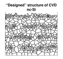
CVD Nanocrystalline Silicon Thermoelectric Material
PatentInactiveUS20160372651A1
Innovation
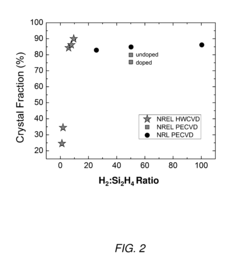
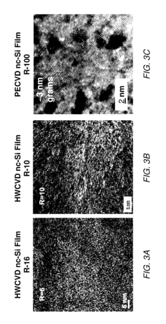
- A three-step process involving the deposition of doped nanocrystalline silicon thin films using hot-wire or plasma-enhanced chemical vapor deposition (CVD) with controlled H2:SiH4 ratios, followed by ion implantation and annealing, to achieve controllable grain sizes and dopant distribution, resulting in a germanium-free thermoelectric material with high electrical conductivity and low thermal conductivity.
Arrays of filled nanostructures with protruding segments and methods thereof
PatentInactiveUS20120152295A1
Innovation
- The development of arrays of filled nanostructures with partially protruding segments, where nanowires or nanostructures are embedded in fill materials and supported by electrodes, enhancing mechanical strength and allowing for efficient heat and energy transfer through increased surface area and thermal gradient support.


Environmental Impact Assessment of TEG Materials
The environmental implications of thermoelectric generator materials represent a critical consideration in the development and deployment of nanostructured TEG systems. Traditional thermoelectric materials often contain toxic or rare elements such as tellurium, bismuth, and lead-based compounds, which pose significant environmental risks throughout their lifecycle from extraction to disposal.
Material toxicity assessment reveals that conventional TEG materials like bismuth telluride and lead telluride present substantial environmental hazards. These compounds can leach into soil and groundwater systems, potentially causing long-term ecological damage. The mining and processing of rare earth elements required for high-performance thermoelectric materials also contribute to environmental degradation through habitat destruction and chemical contamination.
The manufacturing processes for nanostructured thermoelectric materials introduce additional environmental considerations. Synthesis methods often require high-energy consumption and generate chemical waste streams containing organic solvents and metallic residues. Nanoparticle production techniques, while enabling enhanced thermoelectric performance, may release ultrafine particles into the atmosphere during processing, raising concerns about air quality and worker safety.
Lifecycle analysis of TEG systems demonstrates that material selection significantly influences overall environmental impact. While thermoelectric generators offer clean energy conversion during operation, the environmental cost of material production must be weighed against long-term benefits. Studies indicate that TEG systems typically require 3-7 years of operation to offset their manufacturing environmental footprint.
Emerging sustainable alternatives focus on abundant, non-toxic materials such as oxide-based thermoelectrics and organic compounds. Silicon-germanium alloys and magnesium-based materials show promise for reducing environmental impact while maintaining acceptable performance levels. These materials offer improved recyclability and reduced toxicity compared to traditional telluride-based systems.
End-of-life management presents ongoing challenges for TEG materials. Current recycling infrastructure lacks capacity for processing complex nanostructured thermoelectric components. Development of circular economy approaches, including material recovery and reprocessing technologies, remains essential for minimizing long-term environmental impact and ensuring sustainable deployment of thermoelectric energy harvesting systems.
Manufacturing Scalability of Nanostructured TEGs
The manufacturing scalability of nanostructured thermoelectric generators represents one of the most critical barriers to widespread commercial adoption. Current laboratory-scale synthesis methods, while capable of producing high-performance nanostructured materials, face significant challenges when transitioning to industrial-scale production volumes required for commercial viability.
Traditional top-down approaches such as electron beam lithography and focused ion beam milling offer precise control over nanostructure geometry but are inherently limited by throughput constraints and prohibitive costs. These methods typically process single devices or small batches, making them unsuitable for mass production scenarios where millions of units may be required annually.
Bottom-up synthesis techniques present more promising scalability prospects, particularly solution-based methods including hydrothermal synthesis, solvothermal processing, and chemical precipitation. These approaches can potentially achieve large-volume production while maintaining reasonable control over nanostructure morphology and composition. However, maintaining uniformity across large batches remains challenging, as slight variations in reaction conditions can lead to significant performance disparities.
Roll-to-roll processing emerges as a particularly attractive manufacturing pathway for flexible nanostructured TEGs. This continuous production method enables high-throughput fabrication while reducing per-unit costs through economies of scale. Recent developments in printable thermoelectric inks containing nanostructured materials show promise for this approach, though achieving the necessary material densities and electrical connectivity remains technically demanding.
Quality control and characterization present additional scalability challenges. Laboratory-scale devices benefit from extensive individual characterization, but industrial production requires rapid, non-destructive testing methods capable of ensuring consistent performance across large production volumes. Developing inline monitoring systems that can assess nanostructure quality and thermoelectric properties without compromising throughput represents a critical technological gap.
Cost considerations fundamentally drive scalability decisions. While nanostructured materials may offer superior performance, the manufacturing cost premium must be justified by proportional performance improvements or enable access to previously unattainable applications. Economic modeling suggests that production volumes exceeding 100,000 units annually may be necessary to achieve cost parity with conventional thermoelectric devices.
Unlock deeper insights with PatSnap Eureka Quick Research — get a full tech report to explore trends and direct your research. Try now!
Generate Your Research Report Instantly with AI Agent
Supercharge your innovation with PatSnap Eureka AI Agent Platform!