

Optimize Programmable Metasurface Thickness For Maximum Backscattering Control
JUN 4, 202610 MIN READ
Generate Your Research Report Instantly with AI Agent
PatSnap Eureka helps you evaluate technical feasibility & market potential.
Metasurface Backscattering Control Background and Objectives
Metasurfaces represent a revolutionary advancement in electromagnetic wave manipulation, emerging from the fundamental limitations of conventional optical and microwave components. These artificially engineered surfaces consist of subwavelength unit cells that can precisely control electromagnetic wave properties including amplitude, phase, and polarization. The evolution from traditional bulky optical elements to ultrathin metasurfaces has opened unprecedented opportunities for compact, lightweight, and highly efficient electromagnetic devices.
The development trajectory of metasurface technology has progressed from initial theoretical concepts in the early 2000s to sophisticated programmable implementations capable of real-time reconfiguration. Early metasurfaces demonstrated static functionality, while contemporary designs incorporate active elements such as varactors, PIN diodes, and phase-change materials, enabling dynamic control over electromagnetic responses. This evolution has established metasurfaces as critical components in next-generation communication systems, radar applications, and sensing technologies.
Backscattering control represents a particularly crucial application domain for metasurface technology, addressing fundamental challenges in radar cross-section management, wireless communication optimization, and electromagnetic compatibility. The ability to precisely manipulate backscattered electromagnetic waves enables applications ranging from stealth technology to intelligent reflecting surfaces for 6G communications. However, achieving maximum backscattering control requires careful optimization of multiple design parameters, with thickness emerging as a critical factor affecting both performance and practical implementation.
The thickness optimization challenge stems from the inherent trade-off between electromagnetic performance and physical constraints. Thinner metasurfaces offer advantages in terms of weight, integration complexity, and manufacturing costs, while thicker designs potentially provide broader bandwidth and enhanced control capabilities. Current research indicates that optimal thickness selection significantly impacts the achievable backscattering control range, frequency response characteristics, and power handling capabilities.
The primary objective of optimizing programmable metasurface thickness for maximum backscattering control encompasses several key technical goals. These include achieving maximum dynamic range in backscattering coefficient modulation, maintaining stable performance across operational frequency bands, minimizing insertion losses, and ensuring reliable programmability under various environmental conditions. Additionally, the optimization process must consider manufacturing feasibility, cost-effectiveness, and integration requirements with existing systems.
Contemporary research efforts focus on developing comprehensive design methodologies that balance electromagnetic performance with practical implementation constraints, ultimately enabling the realization of highly efficient, compact, and versatile programmable metasurface systems for advanced backscattering control applications.
Market Demand for Advanced Electromagnetic Control Solutions
The global electromagnetic control solutions market is experiencing unprecedented growth driven by the proliferation of wireless communication systems, radar technologies, and emerging applications in autonomous vehicles and IoT devices. The demand for precise electromagnetic wave manipulation has intensified as industries seek to address interference issues, enhance signal quality, and optimize spectrum utilization in increasingly congested electromagnetic environments.
Programmable metasurfaces represent a paradigm shift in electromagnetic control, offering dynamic reconfigurability that traditional passive solutions cannot provide. The telecommunications sector demonstrates particularly strong demand for these technologies, as 5G and beyond-5G networks require sophisticated beamforming capabilities and interference mitigation strategies. Network operators are actively seeking solutions that can adaptively control electromagnetic wave propagation to improve coverage, reduce power consumption, and enhance spectral efficiency.
The defense and aerospace industries constitute another significant market segment, where backscattering control capabilities are crucial for stealth applications and radar cross-section management. Military contractors and defense agencies are investing heavily in metamaterial technologies that can provide real-time electromagnetic signature control, driving demand for optimized metasurface designs with precise thickness parameters.
Automotive manufacturers are emerging as key market drivers, particularly in the development of autonomous vehicles that rely on multiple radar and communication systems. The need for electromagnetic compatibility and interference reduction in these complex sensor environments creates substantial demand for programmable electromagnetic control solutions that can dynamically adapt to changing operational conditions.
The consumer electronics sector also presents growing opportunities, as manufacturers seek to integrate advanced antenna systems and electromagnetic shielding solutions into increasingly compact devices. The miniaturization trend demands metasurface solutions with optimized thickness profiles that can deliver maximum performance within strict spatial constraints.
Market research indicates that the convergence of artificial intelligence with electromagnetic control systems is creating new application domains, including smart building technologies and industrial automation systems. These emerging applications require sophisticated electromagnetic management capabilities that can respond to dynamic environmental conditions and user requirements.
The regulatory landscape is also driving market demand, as governments worldwide implement stricter electromagnetic compatibility standards and spectrum management policies. Organizations must adopt advanced electromagnetic control technologies to ensure compliance while maintaining operational effectiveness, creating sustained demand for innovative metasurface solutions with optimized performance characteristics.
Current State of Programmable Metasurface Thickness Optimization
The current landscape of programmable metasurface thickness optimization represents a rapidly evolving field where researchers are actively pursuing enhanced backscattering control capabilities. Contemporary approaches primarily focus on multi-layer configurations ranging from sub-wavelength thicknesses of λ/10 to several wavelengths, with most practical implementations operating within the λ/4 to λ/2 range to balance performance and fabrication constraints.
Leading research institutions have demonstrated significant progress in developing analytical models for thickness optimization. MIT's recent work has established theoretical frameworks linking substrate thickness to resonance quality factors, while Stanford's electromagnetic simulation studies have validated optimal thickness ranges for specific frequency bands. These foundational studies indicate that thickness optimization directly correlates with achievable phase modulation depth and reflection amplitude control.
Current optimization methodologies predominantly rely on electromagnetic simulation tools such as CST Microwave Studio and ANSYS HFSS, coupled with genetic algorithms and particle swarm optimization techniques. Researchers are implementing multi-objective optimization functions that simultaneously consider backscattering efficiency, bandwidth performance, and manufacturing feasibility. The integration of machine learning approaches, particularly neural networks and reinforcement learning, is emerging as a promising avenue for accelerating the optimization process.
Manufacturing constraints significantly influence current optimization strategies. Photolithography limitations restrict minimum feature sizes to approximately 100 nanometers for most commercial processes, while substrate material properties impose additional thickness-dependent losses. Current fabrication techniques favor discrete thickness levels rather than continuous optimization, leading to quantized design approaches that approximate theoretical optima.
The field faces notable challenges in achieving broadband optimization across multiple frequency ranges simultaneously. Most existing solutions demonstrate optimal performance within narrow bandwidth windows, typically less than 20% fractional bandwidth. Additionally, the trade-off between thickness reduction and scattering efficiency remains a critical limitation, with thinner structures generally exhibiting reduced control authority over electromagnetic wave manipulation.
Recent breakthroughs include the development of gradient-based optimization algorithms specifically tailored for metasurface thickness parameters, enabling more efficient convergence toward optimal solutions. Advanced characterization techniques using near-field scanning and time-domain measurements have provided deeper insights into thickness-dependent electromagnetic behavior, facilitating more accurate optimization models.
Existing Thickness Optimization Methods for Backscattering
01 Tunable thickness control mechanisms for programmable metasurfaces
Methods and systems for dynamically controlling the thickness of programmable metasurfaces through various tuning mechanisms. These approaches enable real-time adjustment of metasurface properties by modifying the physical thickness or effective thickness of the structure. The control mechanisms can include mechanical, electrical, or thermal methods to achieve desired electromagnetic responses.- Tunable thickness control mechanisms for programmable metasurfaces: Methods and systems for dynamically controlling the thickness of metasurface structures through various tuning mechanisms. These approaches enable real-time adjustment of metasurface properties by modifying the physical thickness or effective thickness of the metamaterial layers. The control mechanisms can include mechanical, electrical, or thermal actuation methods that allow for precise thickness modulation to achieve desired electromagnetic responses.
- Multi-layer metasurface thickness optimization: Design strategies for optimizing the thickness distribution across multiple layers in programmable metasurface architectures. These techniques focus on achieving enhanced performance through careful thickness engineering of individual layers and their interactions. The optimization considers factors such as electromagnetic coupling between layers, resonance characteristics, and overall device performance while maintaining programmability features.
- Substrate thickness considerations in programmable metasurfaces: Analysis and design methodologies addressing the impact of substrate thickness on programmable metasurface performance. These approaches examine how substrate properties and dimensions affect the overall electromagnetic behavior and programmability of the metasurface. The considerations include substrate material selection, thickness scaling effects, and integration challenges with active control elements.
- Thickness-dependent electromagnetic response modeling: Computational and analytical methods for modeling the relationship between metasurface thickness and electromagnetic response characteristics. These techniques provide frameworks for predicting and designing thickness-dependent behaviors in programmable metasurfaces. The modeling approaches account for dispersion effects, bandwidth considerations, and the impact of thickness variations on phase and amplitude control capabilities.
- Fabrication techniques for controlled thickness programmable metasurfaces: Manufacturing and fabrication methodologies specifically developed for creating programmable metasurfaces with precise thickness control. These techniques address challenges in achieving uniform thickness distribution, maintaining structural integrity during programming operations, and ensuring reliable performance across different thickness configurations. The methods encompass various deposition, etching, and assembly processes tailored for programmable metasurface applications.
02 Multi-layer thickness optimization for enhanced performance
Techniques for optimizing the thickness distribution across multiple layers in programmable metasurfaces to achieve enhanced electromagnetic performance. This involves careful design of layer thickness ratios and spacing to maximize efficiency while maintaining programmability. The optimization considers both individual layer thickness and overall structure thickness for improved functionality.Expand Specific Solutions03 Substrate thickness considerations in programmable metasurface design
Design methodologies that address the impact of substrate thickness on programmable metasurface performance. These approaches consider how the supporting substrate thickness affects the overall electromagnetic behavior and programmability of the metasurface. The techniques involve optimizing substrate dimensions to minimize interference while maintaining structural integrity.Expand Specific Solutions04 Thickness-dependent frequency response control
Systems and methods for controlling frequency response characteristics through thickness modulation in programmable metasurfaces. These techniques exploit the relationship between structural thickness and electromagnetic resonance to achieve desired frequency selectivity. The approaches enable dynamic frequency tuning by adjusting thickness parameters in real-time.Expand Specific Solutions05 Fabrication methods for precise thickness control
Manufacturing and fabrication techniques specifically designed to achieve precise thickness control in programmable metasurfaces. These methods ensure consistent thickness distribution across the metasurface area while maintaining the ability to program individual elements. The fabrication approaches address challenges related to thickness uniformity and scalability in production.Expand Specific Solutions
Key Players in Metasurface and Electromagnetic Control Industry
The programmable metasurface backscattering control field represents an emerging technology sector in its early-to-mid development stage, characterized by significant research momentum but limited commercial deployment. The market remains relatively nascent with substantial growth potential as applications span telecommunications, radar systems, and electromagnetic wave manipulation. Technology maturity varies considerably across the competitive landscape, with leading Chinese institutions like Zhejiang University, Southeast University, Xidian University, and Harbin Institute of Technology driving fundamental research alongside prestigious international universities including California Institute of Technology and Stanford University. Industrial players such as Huawei Technologies demonstrate commercial interest in practical applications, while specialized equipment manufacturers like ULVAC and Canon Anelva provide essential fabrication tools. Research organizations including Fraunhofer-Gesellschaft and CEA contribute advanced materials science expertise. The field exhibits strong academic-industry collaboration, particularly evident in China's concentrated research efforts, suggesting rapid technological advancement toward practical implementation in next-generation electromagnetic systems and wireless communications infrastructure.
Zhejiang University
Technical Solution: Zhejiang University has developed comprehensive approaches to programmable metasurface thickness optimization, focusing on multi-objective optimization algorithms that balance backscattering control with manufacturing constraints. Their research encompasses both passive and active metasurface designs, utilizing genetic algorithms and particle swarm optimization to determine optimal thickness distributions across metasurface arrays. The university has demonstrated novel approaches using liquid crystal-based tunable metasurfaces where thickness can be dynamically adjusted through voltage control. Their work includes extensive electromagnetic simulation and experimental validation of thickness-optimized designs for applications ranging from radar cross-section reduction to wireless power transfer enhancement.
Strengths: Strong academic research foundation, comprehensive optimization methodologies, extensive simulation capabilities. Weaknesses: Limited industrial partnerships, challenges in transitioning from laboratory to commercial scale production.
Huawei Technologies Co., Ltd.
Technical Solution: Huawei has developed advanced programmable metasurface technologies for wireless communication systems, focusing on intelligent reflecting surfaces (IRS) that can dynamically control electromagnetic wave propagation. Their approach involves multi-layer metasurface designs with optimized thickness parameters to achieve maximum backscattering control for 5G and beyond applications. The company has implemented machine learning algorithms to optimize the phase and amplitude responses of metasurface elements, enabling real-time adaptation of surface properties. Their solutions integrate with existing network infrastructure and provide enhanced signal coverage and interference management through precise control of electromagnetic wave reflection and transmission characteristics.
Strengths: Strong integration with telecommunications infrastructure, extensive R&D resources, practical deployment experience. Weaknesses: Limited focus on non-communication applications, proprietary solutions may lack interoperability.
Core Patents in Programmable Metasurface Thickness Design
Space and polarization multiplexing programmable metasurface
PatentPendingCN117134122A
Innovation
- Design a space and polarization multiplexing programmable metasurface. By integrating varactor diodes and digital voltage control modules on the programmable metasurface, combined with generalized Snell theory and particle swarm optimization algorithm, the deflection direction of the reflected wave can be controlled. , amplitude and phase, achieving polarization state covering any point on the Poincaré sphere.


Programmable metasurface for real time control of broadband elastic rays and method
PatentActiveUS20210327403A1
Innovation
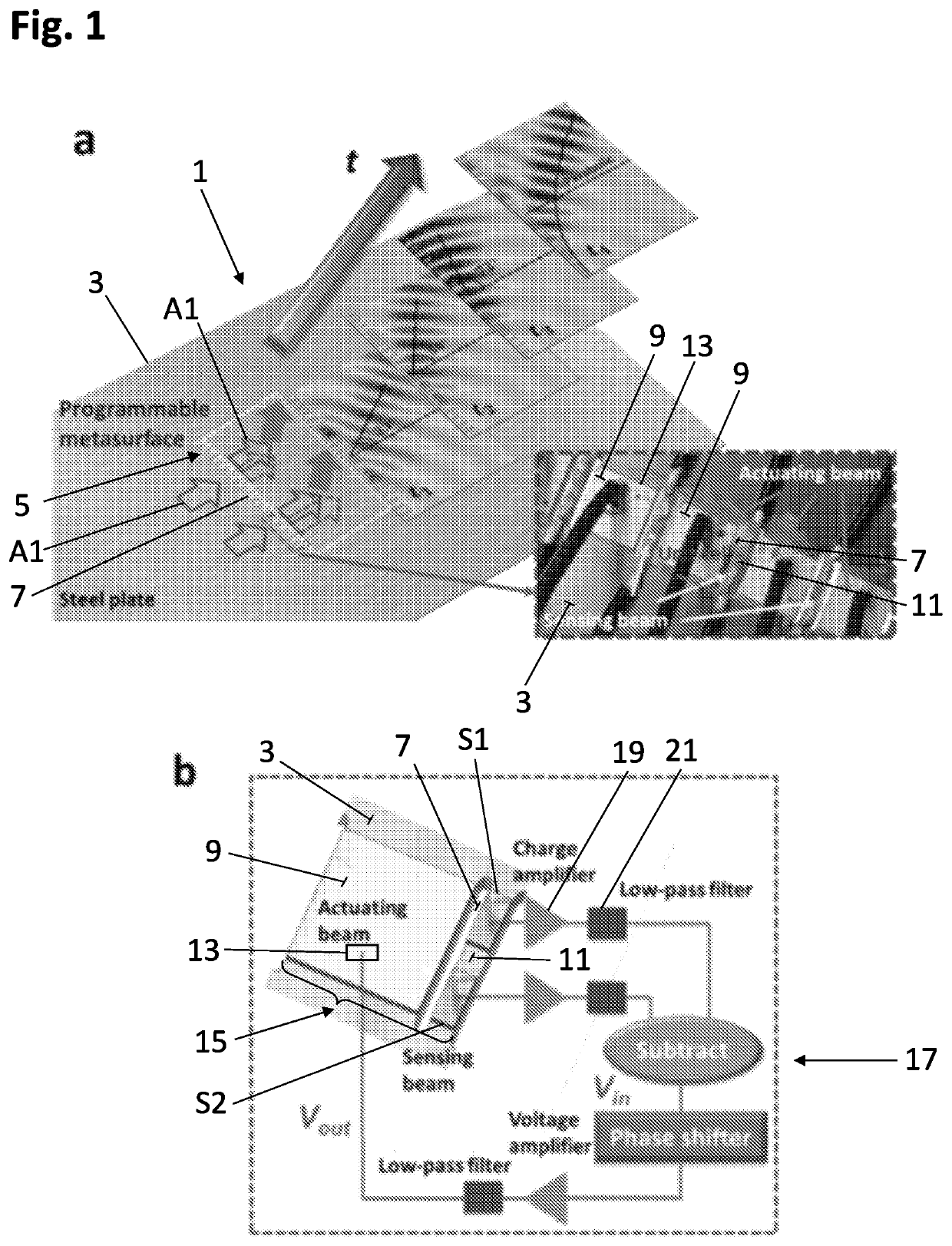
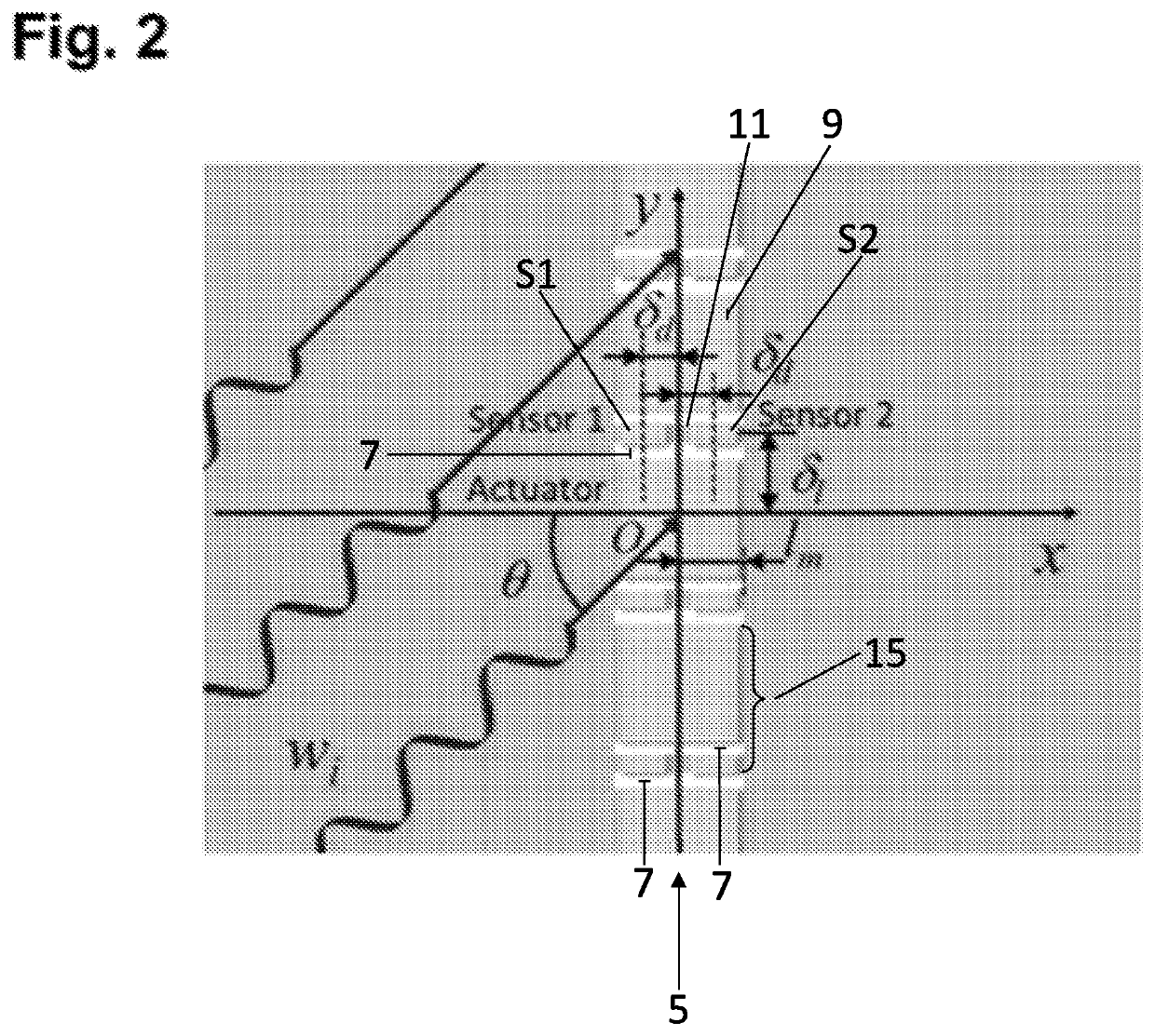
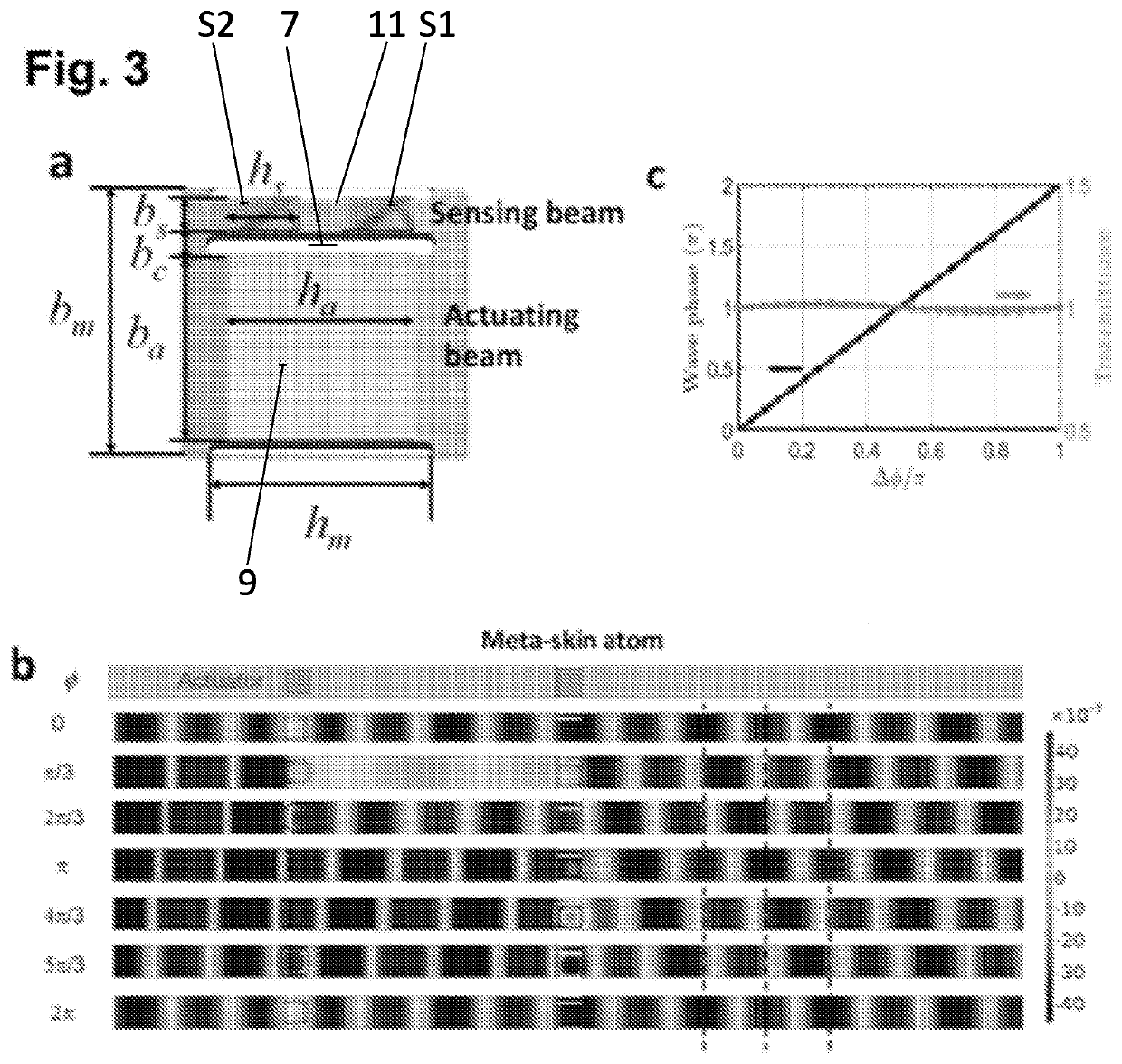
- A programmable elastic metasurface with a 1D array of slits in an elastic plate, featuring self-sensing and self-actuating unit cells with piezoelectric patches, allowing for real-time reconfiguration of wave steering and phase control through digital circuits, enabling multifunctional control of flexural waves across broad frequency ranges.

Electromagnetic Compatibility Standards and Regulations
The development and deployment of programmable metasurfaces for backscattering control must comply with stringent electromagnetic compatibility standards established by international regulatory bodies. The International Electrotechnical Commission (IEC) provides fundamental guidelines through IEC 61000 series standards, which define electromagnetic compatibility requirements for electronic devices operating in various environments. These standards are particularly relevant for metasurface applications as they establish limits for electromagnetic emissions and immunity requirements that directly impact device performance and regulatory approval.
Federal Communications Commission (FCC) regulations in the United States impose specific constraints on electromagnetic emissions from programmable metasurfaces, especially those operating in licensed frequency bands. Part 15 of FCC rules governs unlicensed devices and establishes emission limits that metasurface systems must not exceed. The European Telecommunications Standards Institute (ETSI) provides complementary regulations for European markets, with EN 301 489 series standards addressing electromagnetic compatibility requirements for radio equipment and services.
Military and aerospace applications of programmable metasurfaces face additional regulatory challenges through MIL-STD-461 standards, which specify electromagnetic interference control requirements for defense systems. These standards impose more stringent emission limits and immunity requirements compared to commercial applications, necessitating enhanced shielding and filtering techniques in metasurface design.
Compliance testing protocols require comprehensive electromagnetic compatibility assessments including radiated and conducted emissions measurements, immunity testing against electromagnetic fields, and electrostatic discharge evaluations. Testing must be performed in accredited facilities using standardized measurement procedures defined by CISPR (International Special Committee on Radio Interference) standards.
Regional variations in electromagnetic compatibility requirements create additional complexity for global metasurface deployment. Asian markets follow distinct regulatory frameworks, with Japan's VCCI standards and China's CCC certification requirements imposing unique compliance obligations. These regulatory differences necessitate adaptive design approaches and region-specific testing protocols to ensure market access across different jurisdictions while maintaining optimal backscattering control performance.
Manufacturing Constraints for Ultra-thin Metasurface Devices
The manufacturing of ultra-thin metasurface devices for optimized backscattering control faces significant constraints that directly impact device performance and commercial viability. These limitations stem from the inherent challenges of fabricating structures with nanoscale precision while maintaining electromagnetic functionality across large surface areas.
Lithographic resolution represents the primary bottleneck in metasurface fabrication. Current electron-beam lithography systems can achieve feature sizes below 10 nanometers, but throughput limitations make large-area production economically unfeasible. Photolithography offers higher throughput but is constrained by diffraction limits, typically restricting minimum feature sizes to 100-200 nanometers for cost-effective production. This resolution constraint directly affects the achievable unit cell dimensions and geometric complexity of meta-atoms.
Substrate selection poses another critical manufacturing challenge. Ultra-thin metasurfaces require substrates that provide mechanical stability while minimizing electromagnetic interference. Silicon wafers offer excellent dimensional stability but introduce dielectric losses at higher frequencies. Flexible substrates like polyimide enable conformal applications but suffer from thermal expansion mismatches during processing, leading to pattern distortion and reduced fabrication yield.
Etching precision becomes increasingly critical as device thickness decreases. Aspect ratio limitations in reactive ion etching processes constrain the achievable depth-to-width ratios of metasurface features. For ultra-thin devices operating at terahertz frequencies, maintaining vertical sidewall profiles while achieving etch depths of several hundred nanometers requires careful optimization of plasma chemistry and process parameters.
Material deposition uniformity across large substrates presents scalability challenges. Atomic layer deposition and sputtering techniques can achieve thickness control within 1-2% variation, but maintaining this precision across wafer-scale areas while preserving the optical and electrical properties necessary for backscattering optimization remains technically demanding.
Alignment accuracy between multiple patterning layers becomes critical for complex metasurface designs incorporating multiple materials or multi-layer architectures. Overlay errors exceeding 10% of the minimum feature size can significantly degrade electromagnetic performance, particularly for designs relying on precise geometric relationships between adjacent meta-atoms.
Quality control and metrology present additional constraints. Characterizing ultra-thin metasurface devices requires specialized measurement techniques capable of resolving nanoscale dimensional variations while correlating structural parameters with electromagnetic performance. Scanning electron microscopy provides structural information but cannot directly assess electromagnetic functionality, necessitating complementary optical characterization methods.
These manufacturing constraints collectively define the practical boundaries for ultra-thin metasurface device implementation, requiring careful balance between electromagnetic performance requirements and fabrication feasibility.
Unlock deeper insights with PatSnap Eureka Quick Research — get a full tech report to explore trends and direct your research. Try now!
Generate Your Research Report Instantly with AI Agent
Supercharge your innovation with PatSnap Eureka AI Agent Platform!