Optimizing Scintillator R&D for Speedier Innovations
MAR 10, 20269 MIN READ
Generate Your Research Report Instantly with AI Agent
PatSnap Eureka helps you evaluate technical feasibility & market potential.
Scintillator Technology Background and R&D Goals
Scintillator technology represents a cornerstone of modern radiation detection systems, with applications spanning medical imaging, high-energy physics research, security screening, and nuclear monitoring. These materials convert ionizing radiation into visible light photons, enabling the detection and measurement of various forms of radiation through photodetectors. The fundamental principle relies on the excitation of electrons within the scintillator material, which subsequently emit photons as they return to ground state.
The historical development of scintillators began in the early 20th century with natural materials like zinc sulfide, progressing through organic crystals in the 1940s, and advancing to sophisticated inorganic compounds and plastic scintillators by the 1960s. Modern scintillator research encompasses diverse material categories including single crystals, ceramics, glasses, and nanocomposites, each offering unique advantages for specific applications.
Contemporary scintillator development faces increasing demands for enhanced performance characteristics. The medical imaging sector requires materials with superior light output, faster decay times, and improved energy resolution for advanced CT and PET systems. High-energy physics experiments demand radiation-hard materials capable of withstanding extreme conditions while maintaining detection efficiency. Security applications necessitate cost-effective solutions with high sensitivity for threat detection systems.
Current R&D objectives focus on achieving breakthrough improvements in key performance metrics. Light yield enhancement remains paramount, with researchers targeting materials exceeding 100,000 photons per MeV of absorbed energy. Timing resolution improvements seek sub-nanosecond decay constants for time-of-flight applications. Energy resolution optimization aims for better than 3% at 662 keV gamma energies.
The integration of nanotechnology and advanced materials science opens new pathways for scintillator innovation. Quantum dot incorporation, nanostructured surfaces, and hybrid organic-inorganic compositions represent emerging frontiers. Additionally, the development of transparent ceramics and glass-ceramics offers manufacturing advantages while maintaining superior optical properties.
Accelerating innovation cycles requires systematic approaches to materials discovery, characterization, and optimization. The establishment of standardized testing protocols, computational modeling frameworks, and rapid prototyping capabilities becomes essential for reducing development timelines from years to months while ensuring reliable performance validation across diverse application requirements.
Market Demand for Advanced Scintillator Applications
The global scintillator market is experiencing unprecedented growth driven by expanding applications across multiple high-technology sectors. Medical imaging represents the largest demand segment, with hospitals and diagnostic centers worldwide requiring advanced scintillator materials for computed tomography, positron emission tomography, and digital radiography systems. The aging global population and increasing prevalence of chronic diseases are fueling continuous demand for more sensitive and faster imaging solutions.
Nuclear security and homeland defense applications constitute another rapidly expanding market segment. Government agencies and border control authorities require portable radiation detection systems equipped with high-performance scintillators for threat detection and nuclear material monitoring. The growing concerns about nuclear terrorism and proliferation have intensified procurement activities in this sector.
High-energy physics research facilities represent a specialized but lucrative market niche. Major particle accelerator projects and space-based observatories demand custom scintillator solutions with exceptional radiation hardness and temporal resolution. These applications often drive the development of next-generation materials with superior performance characteristics.
Industrial non-destructive testing markets are increasingly adopting advanced scintillator technologies for quality control and safety inspection applications. Oil and gas exploration, aerospace manufacturing, and infrastructure monitoring sectors require robust detection systems capable of operating in harsh environments while maintaining measurement accuracy.
The emerging quantum technology sector presents significant future opportunities for specialized scintillator applications. Quantum computing research and development programs require ultra-pure scintillator materials with minimal background noise for photon detection and quantum state measurement applications.
Geographically, North America and Europe maintain strong demand driven by established healthcare infrastructure and research institutions. However, Asia-Pacific markets are experiencing the fastest growth rates, particularly in China, Japan, and South Korea, where substantial investments in medical infrastructure and nuclear technology are creating substantial market opportunities for advanced scintillator solutions.
Current Scintillator R&D Challenges and Global Status
The global scintillator research and development landscape faces significant technical and operational challenges that impede rapid innovation cycles. Material synthesis complexity represents a primary bottleneck, as developing new scintillator compositions requires extensive trial-and-error approaches with limited predictive capabilities. Traditional synthesis methods often involve high-temperature processes, complex chemical reactions, and lengthy optimization periods that can extend development timelines by months or years.
Characterization and testing protocols present another substantial challenge. Current evaluation methods for scintillator performance require sophisticated equipment and time-intensive procedures to assess light output, decay time, energy resolution, and radiation hardness. The lack of standardized testing protocols across research institutions creates inconsistencies in performance data, making it difficult to compare results and accelerate collaborative research efforts.
Manufacturing scalability issues significantly constrain the transition from laboratory-scale discoveries to commercial applications. Many promising scintillator materials demonstrate excellent properties in small quantities but face substantial challenges when scaled to industrial production volumes. Quality control becomes increasingly complex as production scales increase, often requiring complete re-optimization of synthesis parameters.
The global distribution of scintillator R&D capabilities reveals distinct regional concentrations and specializations. North America leads in fundamental research and advanced characterization techniques, with major contributions from national laboratories and universities. European institutions excel in crystal growth technologies and specialized applications for high-energy physics experiments. Asian countries, particularly Japan and China, dominate manufacturing capabilities and cost-effective production methods.
Current technological gaps include limited computational modeling tools for predicting scintillator properties, insufficient understanding of defect mechanisms that affect performance, and inadequate integration between materials science and detector system requirements. These challenges collectively contribute to extended development cycles that can span 5-10 years from initial discovery to commercial deployment.
The fragmented nature of the research community further complicates progress, as proprietary concerns and competitive pressures often limit knowledge sharing. This situation is particularly pronounced in commercial applications where intellectual property considerations restrict open collaboration, despite the potential benefits of accelerated innovation through shared research efforts.
Current R&D Optimization Solutions for Scintillators
01 Fast decay time scintillator materials
Development of scintillator materials with rapid decay times to improve detection speed and temporal resolution. These materials enable faster signal processing and higher count rates in radiation detection applications. Advanced crystal compositions and doping techniques are employed to achieve nanosecond-level decay times, which is critical for high-speed imaging and time-of-flight measurements.- Fast decay time scintillator materials: Development of scintillator materials with rapid decay times to improve detection speed and temporal resolution. These materials enable faster signal processing and higher count rates in radiation detection applications. Advanced crystal compositions and doping techniques are employed to achieve nanosecond-level decay times, which is critical for high-speed imaging and particle physics experiments.
- High light yield scintillation crystals: Enhancement of light output efficiency in scintillator crystals to accelerate detection capabilities and improve signal-to-noise ratios. Optimization of crystal growth processes and material purity contributes to increased photon generation per unit of absorbed energy. These improvements enable faster and more sensitive radiation detection systems with reduced measurement times.
- Rapid crystal growth and manufacturing techniques: Advanced manufacturing methods to accelerate the production of scintillator crystals while maintaining quality. Novel growth techniques reduce production time and costs, enabling faster development cycles for scintillator research and commercialization. These methods include improved temperature control, atmosphere optimization, and automated growth processes.
- Composite and ceramic scintillator development: Innovation in composite and ceramic-based scintillators that offer faster fabrication processes compared to traditional single crystal growth. These materials can be produced through sintering, pressing, or casting techniques that significantly reduce manufacturing time. The development enables rapid prototyping and scalable production for various detection applications.
- Optimization of scintillator-photodetector coupling: Improvements in the interface between scintillators and photodetectors to enhance overall system response speed. Advanced coupling materials and geometries minimize light loss and reduce signal transit time. These developments contribute to faster readout electronics and improved temporal resolution in detection systems.
02 High light yield scintillator compositions
Formulation of scintillator materials with enhanced light output to increase detection efficiency and speed. Optimization of crystal structure and activator concentrations results in improved photon generation per unit of absorbed energy. These high-performance materials reduce the time required for signal accumulation and enable faster data acquisition in medical imaging and security screening applications.Expand Specific Solutions03 Ceramic and polycrystalline scintillator fabrication
Manufacturing techniques for producing ceramic and polycrystalline scintillators that offer faster production cycles compared to single crystal growth methods. These approaches utilize sintering and hot pressing processes to create dense scintillator materials with reduced manufacturing time. The technology enables rapid prototyping and scalable production while maintaining adequate optical and scintillation properties.Expand Specific Solutions04 Thin film and nanostructured scintillators
Development of thin film and nanostructured scintillator configurations to achieve faster response times and improved spatial resolution. These architectures minimize light scattering and reduce photon transit time, resulting in enhanced temporal performance. Deposition techniques and nanofabrication methods enable rapid production of scintillator layers with tailored thickness and composition for specific detection applications.Expand Specific Solutions05 Composite and hybrid scintillator systems
Integration of multiple scintillator materials or combination with other detector components to optimize overall detection speed and efficiency. These hybrid systems leverage the complementary properties of different materials to achieve faster signal generation and processing. Advanced coupling techniques and interface engineering enhance light collection efficiency and reduce dead time in detection systems.Expand Specific Solutions
Key Players in Scintillator Research and Manufacturing
The scintillator R&D optimization landscape represents a mature yet rapidly evolving sector driven by increasing demand across medical imaging, security screening, and high-energy physics applications. The market demonstrates significant growth potential, particularly in healthcare diagnostics and industrial inspection systems. Technology maturity varies considerably across the competitive landscape, with established giants like Koninklijke Philips NV, Siemens Medical Solutions, and Canon leading in commercial applications through decades of R&D investment. Japanese specialists including Hamamatsu Photonics and Renesas Electronics contribute advanced photonic detection technologies, while Chinese institutions such as Shanghai Institute of Ceramics and Huazhong University of Science & Technology drive materials innovation. Research institutions like University of Bern and Wake Forest University focus on fundamental scintillator physics, creating a diverse ecosystem spanning from basic research to commercial deployment, indicating a healthy innovation pipeline for accelerated development cycles.
Koninklijke Philips NV
Technical Solution: Philips has developed advanced scintillator materials and detector systems for medical imaging applications, particularly in CT and PET scanners. Their approach focuses on optimizing cesium iodide (CsI) and gadolinium oxysulfide (GOS) scintillators with improved light output and reduced afterglow characteristics. The company has implemented structured CsI scintillators with needle-like crystal growth that provides better spatial resolution and light collection efficiency. Philips has also invested in hybrid scintillator-photodiode detector arrays that enable faster image acquisition and reduced radiation dose for patients. Their R&D efforts include developing new scintillator compositions with enhanced quantum detection efficiency and improved temperature stability for clinical environments.
Strengths: Strong market presence in medical imaging, extensive clinical validation, integrated detector solutions. Weaknesses: Limited focus on non-medical applications, high development costs for regulatory compliance.
Siemens Medical Solutions USA, Inc.
Technical Solution: Siemens has pioneered the development of ultra-fast scintillator materials for next-generation medical imaging systems, focusing on lutetium oxyorthosilicate (LSO) and lutetium yttrium oxyorthosilicate (LYSO) crystals for PET applications. Their innovation pipeline includes novel scintillator geometries and surface treatments that maximize light collection while minimizing cross-talk between detector elements. The company has developed proprietary crystal growth techniques that reduce defects and improve uniformity across large detector arrays. Siemens' approach emphasizes co-optimization of scintillator materials with advanced photodetector technologies, including silicon photomultipliers (SiPMs), to achieve superior timing resolution and energy resolution. Their research extends to exploring perovskite-based scintillators for potential cost reduction and performance enhancement.
Strengths: Advanced crystal growth technology, strong integration capabilities, excellent timing resolution achievements. Weaknesses: High material costs, complex manufacturing processes, limited scalability for mass production.
Core Patents in Accelerated Scintillator Innovation
Solid solution material of rare earth element fluoride (polycrystal and single crystal), and radiation detector and test device
PatentInactiveEP1754808B1
Innovation
- Development of rare earth fluoride solid solution materials by combining rare earth fluorides with controlled ion radii to eliminate phase transitions, incorporating activators like Ce and alkaline earth metals to achieve high emission and short fluorescence lifetimes, and using cost-effective crucible materials for crystal growth.


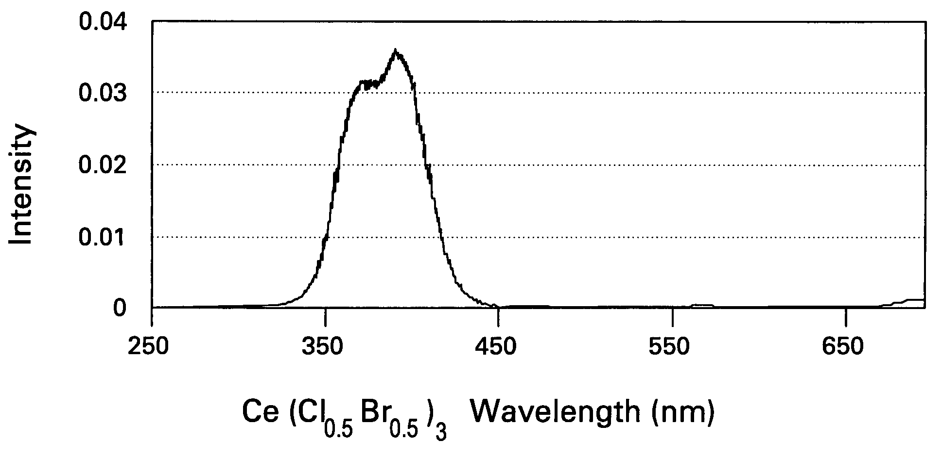
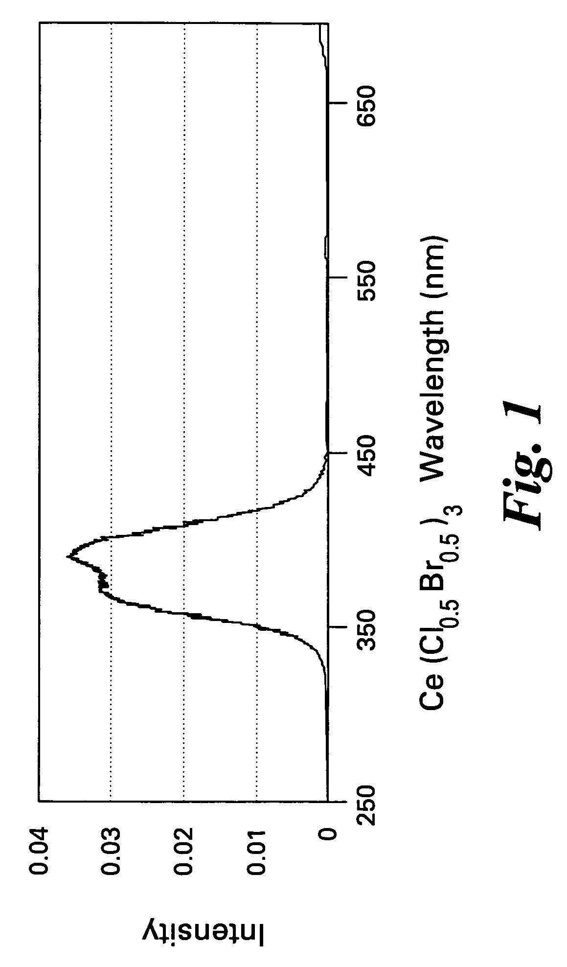
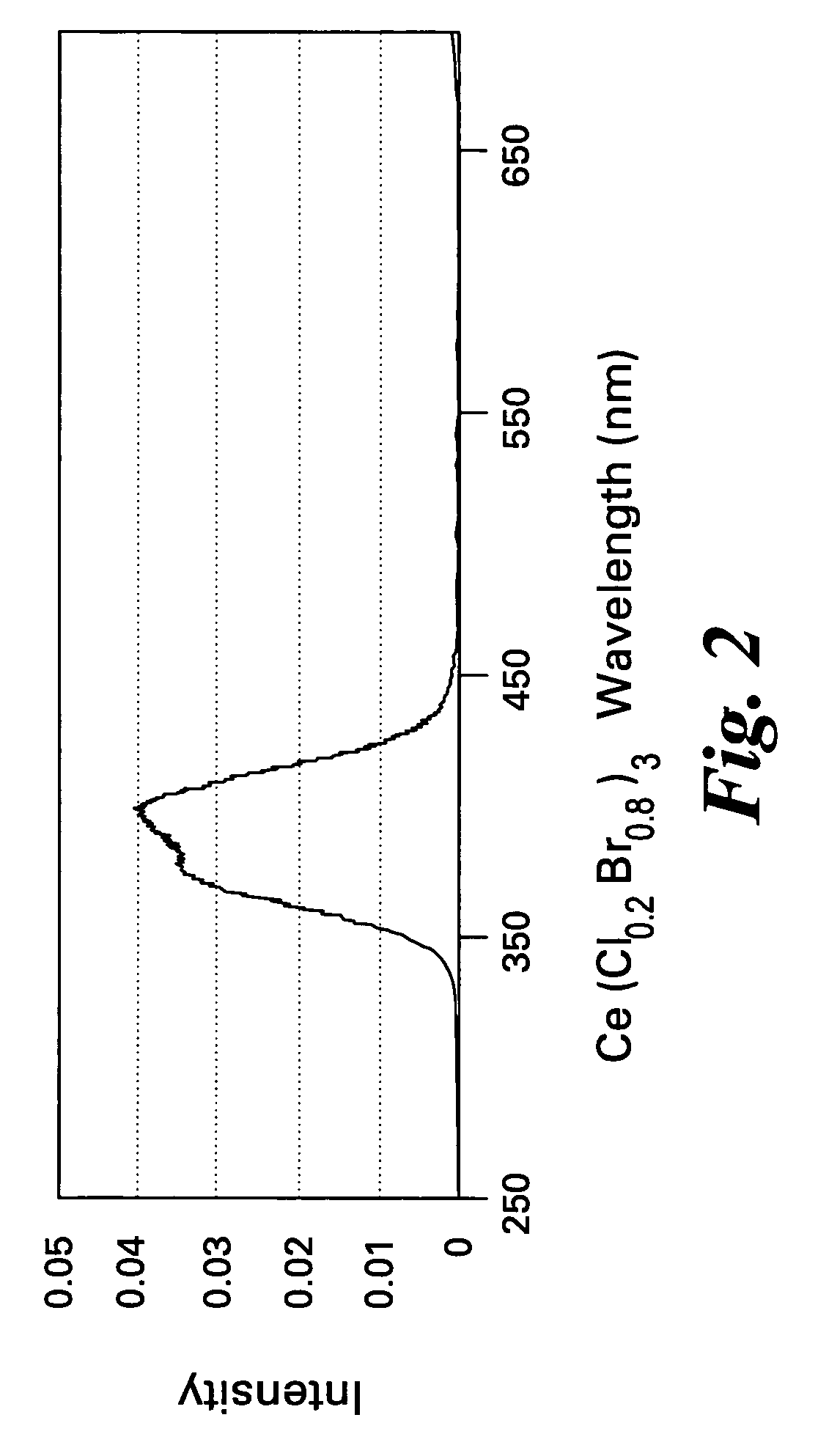
Scintillator compositions of cerium halides, and related articles and processes
PatentInactiveUS7202477B2
Innovation
- A solid solution of cerium halides, specifically cerium chloride and cerium bromide, with optional cerium iodide, is used to form a scintillator composition that is optically coupled with a photodetector to detect high-energy radiation, offering improved light output, decay time, and energy resolution, and can be processed into monocrystalline or polycrystalline forms for various applications.

Material Safety Standards for Scintillator R&D
Material safety standards represent a critical foundation for accelerating scintillator research and development while ensuring researcher protection and regulatory compliance. The complex chemical compositions of modern scintillator materials, ranging from organic crystals to rare earth-doped ceramics, necessitate comprehensive safety protocols that address toxicity, radioactivity, and environmental impact considerations. Establishing robust safety frameworks enables research teams to operate with confidence and efficiency, ultimately contributing to faster innovation cycles.
Current safety standards for scintillator materials are governed by multiple regulatory bodies, including OSHA, EPA, and international organizations such as the International Atomic Energy Agency. These standards encompass handling procedures for toxic compounds like thallium-activated sodium iodide, lead tungstate crystals, and various organic scintillators containing potentially hazardous solvents. The complexity increases when dealing with radioactive materials used in detector calibration and testing, requiring specialized containment and disposal protocols.
The implementation of standardized safety protocols significantly impacts R&D velocity by reducing approval times for new material synthesis and testing procedures. Research institutions that maintain comprehensive safety documentation and training programs experience fewer regulatory delays and can more rapidly transition from laboratory-scale synthesis to prototype development. This streamlined approach is particularly crucial when working with novel nanostructured scintillators or hybrid organic-inorganic materials that may present unknown safety profiles.
Emerging safety considerations include the environmental impact assessment of rare earth mining for scintillator production and the lifecycle management of detector systems. Advanced characterization techniques such as in-situ X-ray diffraction and high-temperature stability testing require specialized safety protocols to protect both personnel and equipment. The development of green chemistry approaches in scintillator synthesis is driving new safety standards that emphasize sustainable material sourcing and waste minimization.
Future safety standard evolution will likely incorporate artificial intelligence-driven risk assessment tools and real-time monitoring systems for laboratory environments. These technological advances promise to further accelerate scintillator R&D by providing predictive safety analytics and automated compliance verification, enabling researchers to focus more resources on innovation rather than administrative safety management.
AI-Driven Approaches in Scintillator Discovery
Artificial intelligence has emerged as a transformative force in scintillator materials discovery, fundamentally reshaping traditional research methodologies. Machine learning algorithms now enable researchers to predict scintillator properties from compositional and structural data, dramatically reducing the time required for initial material screening. These AI-driven approaches leverage vast databases of existing scintillator materials to identify patterns and correlations that would be impossible to detect through conventional analysis methods.
Deep learning models, particularly neural networks, have demonstrated remarkable success in predicting key scintillator characteristics such as light yield, decay time, and energy resolution. Convolutional neural networks excel at analyzing crystal structure data, while recurrent neural networks effectively process time-series data from scintillation decay profiles. These models can rapidly evaluate thousands of potential material combinations, identifying promising candidates for experimental validation within hours rather than months.
High-throughput computational screening powered by AI algorithms has revolutionized the initial phases of scintillator discovery. Density functional theory calculations combined with machine learning models can predict fundamental properties like band gaps, defect formation energies, and optical transitions. This computational approach allows researchers to explore vast chemical spaces systematically, focusing experimental efforts on the most promising material compositions.
Natural language processing techniques are increasingly being applied to extract valuable insights from scientific literature and patent databases. These AI tools can identify emerging trends, correlate material properties with performance metrics, and suggest novel material combinations based on historical research patterns. Such approaches help researchers stay current with rapidly evolving knowledge while identifying unexplored research directions.
Reinforcement learning algorithms represent the cutting edge of AI-driven scintillator discovery, enabling autonomous optimization of material properties through iterative design cycles. These systems can learn from experimental feedback, continuously refining their predictions and suggesting increasingly sophisticated material modifications. The integration of robotic synthesis platforms with AI decision-making creates closed-loop discovery systems that operate with minimal human intervention.
The synergy between AI algorithms and experimental techniques has created unprecedented opportunities for accelerated scintillator development. Real-time analysis of synthesis parameters, automated characterization workflows, and intelligent experiment planning collectively reduce development timelines while improving the quality of discovered materials. This AI-enhanced approach represents a paradigm shift toward data-driven materials science in scintillator research.
Unlock deeper insights with PatSnap Eureka Quick Research — get a full tech report to explore trends and direct your research. Try now!
Generate Your Research Report Instantly with AI Agent
Supercharge your innovation with PatSnap Eureka AI Agent Platform!