

Photonic Computing Systems for Edge AI Applications
MAR 11, 20269 MIN READ
Generate Your Research Report Instantly with AI Agent
PatSnap Eureka helps you evaluate technical feasibility & market potential.
Photonic Computing Background and Edge AI Goals
Photonic computing represents a paradigm shift in computational architecture, leveraging the unique properties of light to perform information processing tasks. Unlike traditional electronic systems that rely on electron movement through semiconductor materials, photonic computing utilizes photons as information carriers, enabling unprecedented speed and energy efficiency. The fundamental principle exploits light's ability to travel at the speed of light in a medium, maintain multiple wavelengths simultaneously, and exhibit minimal crosstalk between parallel channels.
The evolution of photonic computing traces back to the 1960s with the development of lasers and optical fibers, initially focusing on telecommunications applications. Early research concentrated on optical signal processing and analog computing using bulk optics. The 1980s witnessed significant advances in integrated photonics, leading to the development of silicon photonics platforms that enabled miniaturization and mass production compatibility with existing semiconductor fabrication processes.
Modern photonic computing architectures encompass various approaches including coherent optical computing, reservoir computing using photonic neural networks, and hybrid electro-photonic systems. These systems demonstrate remarkable capabilities in matrix multiplication operations, which form the computational backbone of artificial intelligence algorithms. The inherent parallelism of optical systems allows simultaneous processing of multiple data streams through wavelength division multiplexing and spatial multiplexing techniques.
Edge AI applications present unique computational requirements that align exceptionally well with photonic computing capabilities. Edge devices demand ultra-low latency processing for real-time decision making in autonomous vehicles, industrial automation, and augmented reality systems. Traditional electronic processors face fundamental limitations in power consumption and heat dissipation when deployed in resource-constrained edge environments.
The primary objectives for photonic computing in edge AI encompass achieving sub-microsecond inference times for neural network operations while maintaining power consumption below 10 watts per device. These systems must demonstrate scalability across different AI model architectures, from convolutional neural networks for image processing to transformer models for natural language processing tasks.
Integration challenges focus on developing compact, robust photonic processors capable of withstanding environmental variations typical in edge deployment scenarios. The technology aims to enable distributed intelligence networks where edge devices can perform sophisticated AI computations locally, reducing dependence on cloud connectivity and enhancing privacy protection through on-device processing capabilities.
Market Demand for Edge AI Photonic Solutions
The edge AI market is experiencing unprecedented growth driven by the proliferation of IoT devices, autonomous systems, and real-time processing requirements across multiple industries. Traditional electronic processors face significant limitations in power consumption, heat generation, and processing speed when deployed at the edge, creating substantial demand for alternative computing paradigms. Photonic computing systems emerge as a compelling solution to address these fundamental constraints while enabling advanced AI capabilities in resource-constrained environments.
Healthcare applications represent a major demand driver for edge AI photonic solutions, particularly in medical imaging, diagnostic equipment, and wearable health monitors. The ability to process complex neural networks locally while maintaining low power consumption is critical for portable medical devices and implantable systems. Photonic processors can handle the intensive matrix operations required for medical AI algorithms without the thermal management challenges associated with traditional semiconductors.
Autonomous vehicle systems constitute another significant market segment demanding photonic computing capabilities. Real-time sensor fusion, object recognition, and decision-making algorithms require massive parallel processing power with minimal latency. The inherent parallelism of photonic systems aligns perfectly with the computational demands of autonomous driving AI, while their reduced power consumption extends vehicle range and operational efficiency.
Industrial automation and smart manufacturing sectors are increasingly adopting edge AI solutions for predictive maintenance, quality control, and process optimization. Photonic computing systems offer the computational density needed to run sophisticated AI models directly on factory floors, enabling immediate response to anomalies without relying on cloud connectivity. The harsh industrial environments also benefit from the electromagnetic interference immunity inherent in photonic systems.
Telecommunications infrastructure modernization drives substantial demand for edge AI photonic solutions, particularly in 5G and beyond networks. Network optimization, traffic management, and security applications require distributed AI processing capabilities that can handle massive data throughput while maintaining energy efficiency. Photonic processors naturally integrate with optical communication systems, reducing conversion overhead and improving overall network performance.
The defense and aerospace sectors present specialized but high-value market opportunities for photonic edge AI systems. Applications include radar signal processing, electronic warfare, and satellite communications where size, weight, power, and performance constraints are critical. The radiation hardness and electromagnetic compatibility of photonic systems provide additional advantages in these demanding environments.
Current State of Photonic Computing for Edge Applications
Photonic computing for edge AI applications has emerged as a promising paradigm that leverages light-based processing to overcome the computational and energy limitations of traditional electronic systems. Current implementations primarily focus on optical neural network accelerators that utilize photonic integrated circuits (PICs) to perform matrix-vector multiplications and convolution operations essential for deep learning inference tasks.
The technology landscape is dominated by silicon photonics platforms, which offer compatibility with existing semiconductor manufacturing processes. Leading research institutions and companies have demonstrated functional prototypes capable of performing inference tasks for convolutional neural networks and transformer models. These systems typically operate in the near-infrared wavelength range, utilizing wavelength division multiplexing (WDM) and intensity modulation schemes to encode and process data.
Performance benchmarks indicate that current photonic computing systems can achieve energy efficiencies of 1-10 TOPS/W for specific AI workloads, representing significant improvements over conventional GPU-based solutions. However, these systems are primarily optimized for linear operations and face challenges in implementing non-linear activation functions, which are typically handled by electronic components in hybrid architectures.
The integration density remains a critical limitation, with current photonic processors supporting neural networks with hundreds to thousands of parameters, significantly smaller than state-of-the-art electronic AI accelerators. Precision is another constraint, as most demonstrations operate with 4-8 bit resolution, which may limit accuracy for certain applications but proves sufficient for many edge inference tasks.
Manufacturing maturity varies significantly across different photonic platforms. Silicon photonics has reached relatively high technology readiness levels with established foundry services, while emerging platforms like lithium niobate and III-V semiconductors remain largely in research phases. The packaging and integration of photonic components with electronic control systems present ongoing engineering challenges that impact system reliability and cost-effectiveness.
Current commercial deployments are limited to specialized applications in telecommunications and data centers, with edge AI applications still primarily in prototype and pilot phases. The technology demonstrates particular promise for applications requiring high-throughput, low-latency processing such as autonomous vehicles, industrial automation, and real-time video analytics, where the inherent parallelism and speed of light propagation provide distinct advantages over electronic alternatives.
Existing Photonic Edge AI Solutions
01 Optical neural network architectures for photonic computing
Photonic computing systems can utilize optical neural network architectures that leverage light-based components to perform computational tasks. These systems employ optical elements such as waveguides, modulators, and photodetectors to implement neural network operations. The optical approach enables parallel processing and high-speed computation while reducing power consumption compared to traditional electronic systems. Various configurations of optical layers and interconnections can be designed to optimize performance for specific computational tasks.- Optical neural network architectures and photonic tensor processing: Photonic computing systems utilize optical neural networks that perform matrix operations and tensor computations using light-based components. These architectures employ photonic integrated circuits with optical modulators, waveguides, and photodetectors to implement neural network layers. The systems leverage the parallelism of optics to perform high-speed matrix multiplications and convolutions, enabling efficient deep learning inference and training with reduced power consumption compared to electronic counterparts.
- Photonic quantum computing and quantum information processing: Advanced photonic systems implement quantum computing operations using photonic qubits and quantum gates. These systems utilize single photons, squeezed light states, and entangled photon pairs to perform quantum algorithms. The architectures include photonic quantum processors with integrated optical components for generating, manipulating, and measuring quantum states of light, enabling applications in quantum simulation, optimization, and cryptography.
- Integrated photonic chip design and silicon photonics platforms: Photonic computing implementations utilize integrated photonic chips fabricated on silicon or other substrates. These platforms integrate multiple optical components including lasers, modulators, switches, and detectors on a single chip. The designs employ wavelength division multiplexing, mode division multiplexing, and advanced coupling structures to achieve high-density integration and scalability for large-scale photonic computing systems.
- Optical interconnects and data transmission in photonic processors: Photonic computing systems employ optical interconnect technologies for high-bandwidth, low-latency data communication between processing elements. These systems utilize optical waveguides, fiber optics, and free-space optical links to transmit data signals. The architectures implement advanced modulation schemes, wavelength routing, and optical switching to enable efficient data flow and reduce bottlenecks in distributed photonic computing networks.
- Hybrid photonic-electronic computing architectures: Computing systems integrate both photonic and electronic components to leverage the advantages of each technology. These hybrid architectures use photonic elements for high-speed parallel processing and optical data transmission, while electronic circuits handle control logic, memory operations, and digital signal processing. The systems employ efficient conversion interfaces between optical and electrical domains to optimize overall performance and energy efficiency for various computing workloads.
02 Integrated photonic circuits and chip-scale implementations
Photonic computing systems can be implemented using integrated photonic circuits that combine multiple optical components on a single chip. These chip-scale implementations utilize silicon photonics or other material platforms to create compact and scalable computing devices. The integration approach allows for miniaturization of photonic computing elements while maintaining high performance. Manufacturing techniques from semiconductor industry can be adapted to produce these integrated photonic computing chips at scale.Expand Specific Solutions03 Quantum photonic computing and quantum information processing
Advanced photonic computing systems can incorporate quantum mechanical principles to perform quantum information processing. These systems utilize quantum states of light, such as single photons or entangled photon pairs, to implement quantum algorithms and computations. Quantum photonic approaches offer potential advantages for specific computational problems including cryptography, optimization, and simulation. The systems require specialized components for generating, manipulating, and detecting quantum states of light.Expand Specific Solutions04 Optical interconnects and data transmission in photonic systems
Photonic computing systems employ optical interconnects to enable high-bandwidth data transmission between computing elements. These interconnects use light signals propagating through optical waveguides or free space to transfer information with minimal latency and energy loss. The optical data transmission approach overcomes bandwidth limitations of electrical interconnects and reduces signal degradation. Various modulation schemes and multiplexing techniques can be implemented to maximize data throughput in photonic computing architectures.Expand Specific Solutions05 Hybrid photonic-electronic computing architectures
Photonic computing systems can be designed as hybrid architectures that combine both photonic and electronic components to leverage advantages of each technology. These systems integrate optical processing elements with electronic control circuits and memory units to create versatile computing platforms. The hybrid approach allows for efficient interfacing with existing electronic infrastructure while exploiting the speed and parallelism of photonic processing. Control algorithms and system architectures can be optimized to balance workload distribution between photonic and electronic subsystems.Expand Specific Solutions
Key Players in Photonic Computing Industry
The photonic computing systems for edge AI applications market represents an emerging technology sector in its early commercialization phase, with significant growth potential driven by increasing demand for energy-efficient AI processing at network edges. The market remains relatively nascent but shows promising expansion as organizations seek alternatives to traditional electronic computing for AI workloads. Technology maturity varies considerably across players, with established companies like Intel Corp., Taiwan Semiconductor Manufacturing Co., and Lightmatter Inc. leading advanced development efforts, while research institutions including Tsinghua University, University of Washington, and Southeast University contribute foundational innovations. Specialized photonics companies such as Artilux Inc. and emerging players like Zhejiang Lab are developing targeted solutions, though most technologies remain in prototype or early deployment stages, indicating substantial room for market evolution and competitive positioning.
Lightmatter, Inc.
Technical Solution: Lightmatter develops photonic computing systems that use light instead of electrons for data processing and interconnects. Their Passage interconnect technology enables high-bandwidth, low-latency communication between AI processors, achieving up to 10x improvement in energy efficiency compared to traditional electronic interconnects. The company's photonic neural network accelerators leverage wavelength division multiplexing and optical matrix multiplication to perform AI computations at the speed of light, significantly reducing power consumption and heat generation. Their systems are specifically designed for edge AI applications where power efficiency and thermal management are critical constraints. The technology integrates silicon photonics with CMOS electronics to create hybrid computing platforms that can handle complex AI workloads while maintaining compact form factors suitable for edge deployment.
Strengths: Ultra-low power consumption, high-speed optical processing, excellent thermal management. Weaknesses: Limited programmability, high manufacturing complexity, sensitivity to environmental conditions.
Huawei Technologies Canada Co. Ltd.
Technical Solution: Huawei has developed photonic computing solutions that integrate optical processing with their existing AI chip architectures for edge applications. Their approach focuses on optical interconnects and photonic accelerators that can be deployed in edge computing scenarios such as 5G base stations and autonomous driving systems. The company's photonic technology includes optical switching networks that enable high-bandwidth, low-latency communication between distributed AI processing units, as well as optical neural network accelerators that perform convolution operations using integrated photonic circuits. Huawei's edge AI photonic systems are designed to handle real-time inference tasks with strict power and thermal constraints, utilizing silicon photonics technology to achieve high computational density while maintaining energy efficiency. Their solutions integrate with their Ascend AI processors to create hybrid electronic-photonic computing platforms optimized for edge deployment scenarios.
Strengths: Integration with existing AI ecosystem, focus on practical edge applications, strong system-level optimization. Weaknesses: Limited availability in some markets due to trade restrictions, relatively new to photonic computing field.
Core Photonic Computing Patents and Innovations
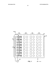
Photonic neural network
PatentWO2020247391A1
Innovation
- A photonic neural network device featuring a planar waveguide with a layer of changeable refractive index and programmable electrodes that apply configurable voltages to induce amplitude or phase modulation of light, enabling reconfigurable and scalable neural network architectures with thousands of neurons and connections.

Photonic Neural Network
PatentPendingUS20250384260A1
Innovation
- A programmable photonic computer system that utilizes silicon photonics to integrate optical waveguides, phase shifters, and photodetectors, eliminating nonlinear devices and implementing data reuploading to achieve universal non-quantum photonic computing, mimicking classical neural networks without cryogenics.


Energy Efficiency Standards for Edge Computing
The integration of photonic computing systems into edge AI applications necessitates the establishment of comprehensive energy efficiency standards that address the unique characteristics of optical processing architectures. Current energy efficiency metrics primarily designed for electronic systems fail to adequately capture the power consumption patterns and operational dynamics of photonic processors, which exhibit fundamentally different energy profiles during computation and idle states.
Photonic computing systems demonstrate exceptional energy efficiency advantages in specific computational tasks, particularly matrix operations and neural network inference, where optical signal processing can achieve orders of magnitude lower energy consumption compared to traditional electronic counterparts. However, the absence of standardized measurement protocols creates significant challenges in quantifying and comparing energy performance across different photonic architectures and deployment scenarios.
The development of energy efficiency standards for photonic edge computing must consider several critical factors unique to optical systems. These include the energy overhead associated with electro-optical conversions, the power requirements for laser sources and optical modulators, and the thermal management needs of photonic integrated circuits. Unlike purely electronic systems, photonic processors often maintain baseline power consumption for optical source stability, requiring new metrics that account for both active computation and standby power states.
Industry stakeholders are actively working toward establishing unified benchmarking frameworks that incorporate photonic-specific parameters such as optical power budgets, wavelength division multiplexing efficiency, and photonic memory access patterns. These standards must also address the scalability aspects of photonic systems, where energy efficiency can vary significantly based on the complexity of optical interconnects and the degree of integration between photonic and electronic components.
The proposed energy efficiency standards should encompass standardized testing methodologies, performance metrics that reflect real-world edge computing workloads, and certification processes that enable fair comparison between photonic and conventional computing solutions. This standardization effort is crucial for accelerating the adoption of photonic computing in edge AI applications while ensuring optimal energy utilization across diverse deployment environments.
Integration Challenges with Silicon Electronics
The integration of photonic computing systems with silicon electronics presents multifaceted challenges that significantly impact the deployment of edge AI applications. The fundamental disparity between optical and electronic signal processing creates complex interface requirements that must be carefully addressed to achieve seamless system operation.
Signal conversion represents the most critical integration challenge, as photonic processors operate with optical signals while silicon-based components process electrical signals. This necessitates sophisticated electro-optical and opto-electrical conversion interfaces that introduce latency, power consumption, and potential signal degradation. The conversion overhead can significantly impact the overall system performance, particularly in edge AI applications where real-time processing is essential.
Thermal management emerges as another significant challenge due to the different thermal characteristics of photonic and electronic components. Silicon electronics generate substantial heat during operation, while photonic devices are highly sensitive to temperature variations that can affect their optical properties and performance stability. Maintaining optimal operating temperatures for both subsystems requires advanced thermal design strategies and potentially increases system complexity.
Physical packaging and interconnect design pose substantial engineering challenges. Photonic components require precise optical alignment and protection from environmental factors, while silicon electronics demand efficient electrical connectivity and electromagnetic interference shielding. The hybrid packaging solutions must accommodate both requirements without compromising performance or reliability.
Manufacturing compatibility issues arise from the different fabrication processes required for photonic and silicon components. Standard CMOS fabrication techniques are well-established for silicon electronics, but integrating photonic elements often requires specialized materials and processing steps that may not be fully compatible with existing semiconductor manufacturing infrastructure.
Power distribution and management become increasingly complex in hybrid systems. Photonic components typically require different voltage levels and power characteristics compared to silicon electronics. Designing efficient power delivery networks that serve both subsystems while minimizing interference and maintaining power efficiency presents significant engineering challenges.
Synchronization and timing coordination between optical and electrical domains require sophisticated control mechanisms. The different propagation characteristics and processing speeds of photonic and electronic signals necessitate careful timing management to ensure proper system operation and data integrity in edge AI applications.
Unlock deeper insights with PatSnap Eureka Quick Research — get a full tech report to explore trends and direct your research. Try now!
Generate Your Research Report Instantly with AI Agent
Supercharge your innovation with PatSnap Eureka AI Agent Platform!