

Photonic Signal Processing for High-Speed AI Models
MAR 11, 20269 MIN READ
Generate Your Research Report Instantly with AI Agent
PatSnap Eureka helps you evaluate technical feasibility & market potential.
Photonic AI Processing Background and Objectives
Photonic signal processing represents a paradigm shift in computational architectures, leveraging the unique properties of light to overcome the fundamental limitations of electronic systems. As artificial intelligence models continue to scale exponentially in complexity and parameter count, traditional electronic processors face insurmountable bottlenecks in terms of power consumption, heat dissipation, and processing speed. The emergence of transformer architectures, large language models, and deep neural networks has created an urgent demand for computational platforms capable of handling massive parallel operations at unprecedented speeds.
The evolution of photonic computing traces back to early optical computing research in the 1960s, where scientists first explored using light for information processing. However, recent breakthroughs in silicon photonics, integrated optical circuits, and advanced materials have transformed photonic processing from theoretical concepts into practical solutions. The convergence of mature semiconductor fabrication techniques with photonic device manufacturing has enabled the development of scalable, cost-effective optical processing units specifically designed for AI workloads.
Current electronic AI accelerators, while powerful, are constrained by the von Neumann bottleneck and the physical limitations of electron-based computation. Heat generation, signal degradation, and interconnect delays become increasingly problematic as model sizes grow. Photonic systems offer inherent advantages including massive parallelism through wavelength division multiplexing, near-zero latency signal propagation at light speed, and minimal power consumption for data transmission across optical waveguides.
The primary objective of photonic signal processing for high-speed AI models centers on developing integrated photonic circuits capable of performing matrix-vector multiplications, convolutions, and other fundamental AI operations directly in the optical domain. This approach aims to achieve computational throughput improvements of several orders of magnitude while dramatically reducing energy consumption per operation. Key technical goals include implementing reconfigurable optical neural networks, developing efficient optical-electronic interfaces, and creating scalable architectures that can accommodate the growing complexity of modern AI models.
Furthermore, the technology seeks to enable real-time processing of high-bandwidth data streams, particularly beneficial for applications in autonomous systems, real-time video analysis, and edge computing scenarios where latency and power efficiency are critical. The ultimate vision encompasses fully integrated photonic AI processors that can seamlessly interface with existing electronic systems while providing unprecedented computational capabilities for next-generation artificial intelligence applications.
Market Demand for High-Speed AI Computing Solutions
The global artificial intelligence computing market is experiencing unprecedented growth driven by the exponential increase in data generation and the complexity of AI models. Traditional electronic processors face fundamental limitations in bandwidth, power consumption, and processing speed when handling large-scale neural networks and real-time inference tasks. This creates a substantial market opportunity for photonic signal processing solutions that can overcome these bottlenecks.
Data centers and cloud computing providers represent the largest segment of demand for high-speed AI computing solutions. These facilities require massive parallel processing capabilities to support machine learning training workloads, natural language processing, and computer vision applications. The energy efficiency advantages of photonic processors become particularly compelling at scale, where power consumption directly impacts operational costs and environmental sustainability goals.
Edge computing applications constitute another rapidly expanding market segment. Autonomous vehicles, industrial automation systems, and smart city infrastructure demand real-time AI processing with minimal latency. Photonic signal processing offers the potential to perform complex computations at the speed of light, enabling instantaneous decision-making in safety-critical applications where millisecond delays can have significant consequences.
The telecommunications industry presents substantial opportunities as 5G and future 6G networks require advanced signal processing capabilities. Network function virtualization and software-defined networking rely heavily on AI algorithms for traffic optimization, resource allocation, and predictive maintenance. Photonic processors can handle the massive data throughput requirements while maintaining low latency for real-time network management.
Financial services and high-frequency trading represent specialized but lucrative market segments. These applications demand ultra-low latency processing for algorithmic trading, risk analysis, and fraud detection. The speed advantages of photonic computing can provide competitive advantages measured in microseconds, translating to significant financial value.
Healthcare and life sciences applications are emerging as important growth areas. Medical imaging, drug discovery, and genomic analysis require intensive computational resources for AI model inference. Photonic processors can accelerate these workflows while reducing the time-to-insight for critical medical applications.
The market demand is further amplified by the increasing adoption of transformer-based models and large language models that require substantial computational resources. Organizations across industries are seeking solutions that can handle these demanding workloads efficiently while managing infrastructure costs and energy consumption.
Current State of Photonic Signal Processing Technologies
Photonic signal processing has emerged as a transformative technology for addressing the computational demands of high-speed AI models, leveraging the unique properties of light to perform complex mathematical operations at unprecedented speeds. Current implementations primarily utilize silicon photonics platforms, which integrate optical components with traditional semiconductor manufacturing processes, enabling scalable production of photonic processors.
The technology landscape is dominated by several key approaches, including coherent optical computing systems that exploit interference patterns for matrix multiplication operations, and incoherent systems that utilize intensity-based calculations. Major research institutions and companies have demonstrated photonic tensor processing units capable of performing convolution operations at terahertz frequencies, significantly outpacing electronic counterparts in specific computational tasks.
Silicon photonic platforms currently represent the most mature technology, with companies successfully implementing Mach-Zehnder interferometer arrays for neural network acceleration. These systems achieve remarkable energy efficiency improvements, consuming orders of magnitude less power per operation compared to traditional GPU-based solutions. However, current implementations face limitations in precision, typically operating with 4-8 bit resolution due to optical noise and fabrication tolerances.
Emerging technologies include integrated photonic circuits utilizing lithium niobate and indium phosphide substrates, which offer superior electro-optic properties but at higher manufacturing costs. Recent breakthroughs in photonic memory systems have enabled on-chip weight storage using phase-change materials, addressing one of the critical bottlenecks in photonic AI acceleration.
The current state reveals significant progress in specialized applications such as convolutional neural networks for image processing and transformer architectures for natural language processing. However, challenges persist in achieving the flexibility and programmability required for general-purpose AI workloads. Manufacturing scalability remains a critical constraint, with most current systems limited to research-scale implementations rather than commercial deployment.
Despite these limitations, the technology demonstrates clear advantages in specific high-throughput, low-latency applications, positioning photonic signal processing as a complementary rather than replacement technology for existing electronic AI accelerators.
Existing Photonic Signal Processing Architectures
01 High-speed optical signal processing using photonic integrated circuits
Photonic integrated circuits enable high-speed signal processing by integrating multiple optical components on a single chip. These circuits can process optical signals at speeds significantly higher than traditional electronic circuits by eliminating electrical-to-optical conversions. The integration of waveguides, modulators, and detectors on a single substrate reduces signal propagation delays and enables parallel processing of multiple optical channels simultaneously.- High-speed optical signal processing using photonic integrated circuits: Photonic integrated circuits enable high-speed signal processing by integrating multiple optical components on a single chip. These circuits can process optical signals at speeds significantly higher than traditional electronic circuits by eliminating electrical-to-optical conversions. The integration of waveguides, modulators, and detectors on a single platform reduces signal propagation delays and increases overall processing throughput.
- Parallel processing architectures for photonic signal processing: Parallel processing techniques utilize multiple optical channels simultaneously to increase the overall processing speed. By dividing signals across multiple wavelengths or spatial channels, these architectures can achieve higher data throughput rates. The parallel nature of optical processing allows for simultaneous operations on different signal components, significantly reducing processing time compared to sequential methods.
- Wavelength division multiplexing for enhanced processing speed: Wavelength division multiplexing techniques enable multiple signals to be processed simultaneously on different wavelength channels within the same optical medium. This approach increases the aggregate processing speed by allowing parallel operations on multiple wavelength channels. The technology leverages the broad bandwidth of optical fibers to carry multiple independent data streams, each operating at high speeds.
- Ultrafast optical switching and modulation technologies: Advanced optical switching and modulation technologies enable rapid signal manipulation at picosecond or femtosecond timescales. These technologies utilize nonlinear optical effects, electro-optic materials, or all-optical switching mechanisms to achieve ultrafast signal processing speeds. The elimination of electronic bottlenecks allows for processing rates that exceed traditional electronic systems by orders of magnitude.
- Optical signal processing with reduced latency through direct photonic manipulation: Direct photonic manipulation techniques process optical signals without conversion to electrical domain, thereby minimizing latency and increasing processing speed. These methods employ optical logic gates, optical correlators, and photonic neural networks to perform computations directly in the optical domain. The approach eliminates conversion delays and enables real-time processing of high-bandwidth optical signals.
02 Wavelength division multiplexing for increased processing throughput
Wavelength division multiplexing technology enables simultaneous processing of multiple optical signals at different wavelengths through a single optical fiber or waveguide. This approach significantly increases the overall processing speed and data throughput by allowing parallel processing of independent data streams. The technique utilizes optical filters and demultiplexers to separate and process different wavelength channels independently before recombining them.Expand Specific Solutions03 Optical switching and routing for reduced latency
Advanced optical switching mechanisms enable rapid routing and redirection of photonic signals without electrical conversion, significantly reducing processing latency. These systems employ various switching technologies including micro-electromechanical systems, liquid crystal devices, and semiconductor optical amplifiers to achieve nanosecond-scale switching times. The elimination of optical-electrical-optical conversions in the signal path enables faster processing and lower power consumption.Expand Specific Solutions04 Parallel optical processing architectures
Parallel processing architectures utilizing multiple optical channels enable simultaneous processing of data streams to achieve higher overall processing speeds. These architectures employ spatial light modulators, optical correlators, and array detectors to process multiple data elements concurrently. The inherent parallelism of optical systems allows for massive parallel operations that would be difficult to achieve with electronic circuits alone.Expand Specific Solutions05 Ultrafast optical modulation and detection techniques
Advanced modulation and detection techniques enable processing of optical signals at extremely high speeds by utilizing ultrafast optical phenomena. These techniques include electro-optic modulation, all-optical switching, and high-speed photodetection that can operate at frequencies exceeding hundreds of gigahertz. The use of novel materials and device structures enables faster response times and higher bandwidth capabilities for signal processing applications.Expand Specific Solutions
Key Players in Photonic AI and Optical Computing Industry
The photonic signal processing market for high-speed AI models represents an emerging technology sector in its early commercialization phase, with significant growth potential driven by the increasing demand for faster, more energy-efficient AI computing solutions. The market is currently valued in the hundreds of millions but is projected to reach multi-billion dollar scale as AI workloads continue to expand exponentially. Technology maturity varies significantly across players, with specialized photonics companies like Lightmatter and Shanghai Xizhi Technology leading in dedicated photonic AI processors, having demonstrated functional prototypes and early commercial products. Established semiconductor giants including Samsung Electronics, Sony Semiconductor Solutions, and Qualcomm are investing heavily in photonic integration research, while traditional tech companies such as Baidu and NEC are exploring photonic solutions for their AI infrastructure needs. Academic institutions like Shanghai Jiao Tong University and Tianjin University contribute fundamental research, though the technology remains in early stages with challenges in manufacturing scalability and integration with existing electronic systems still being addressed.
Samsung Electronics Co., Ltd.
Technical Solution: Samsung has developed advanced photonic integration technologies for high-speed signal processing applications. Their approach focuses on silicon photonics platforms that integrate optical modulators, photodetectors, and waveguides on a single chip for AI acceleration. The company leverages their semiconductor manufacturing expertise to create hybrid electronic-photonic systems that can handle high-bandwidth data processing required for large-scale AI models. Samsung's technology incorporates advanced packaging solutions that enable efficient coupling between electronic and photonic components, facilitating seamless data transfer and processing. Their photonic signal processing solutions target data center applications where high-speed interconnects and parallel processing capabilities are essential for AI workloads.
Advantages: Strong manufacturing capabilities, proven semiconductor expertise, scalable production infrastructure. Disadvantages: Still in early development stages, limited commercial availability, requires significant R&D investment.
Lightmatter, Inc.
Technical Solution: Lightmatter develops photonic computing platforms that utilize light-based interconnects and processing units for AI acceleration. Their technology employs silicon photonics to create optical neural networks that can process data at the speed of light with significantly reduced power consumption. The company's photonic processors integrate wavelength division multiplexing (WDM) to enable parallel processing of multiple data streams simultaneously. Their approach combines traditional electronic computing with photonic signal processing, allowing for matrix-vector multiplications to be performed optically, which is fundamental for neural network operations. The system achieves substantial improvements in bandwidth density and energy efficiency compared to traditional electronic processors.
Advantages: Ultra-low latency processing at light speed, dramatically reduced power consumption, high bandwidth density through WDM technology. Disadvantages: Limited to specific AI operations, requires specialized cooling systems, high manufacturing complexity and costs.
Core Innovations in Optical Neural Network Processing
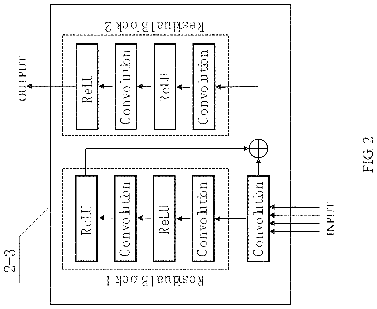
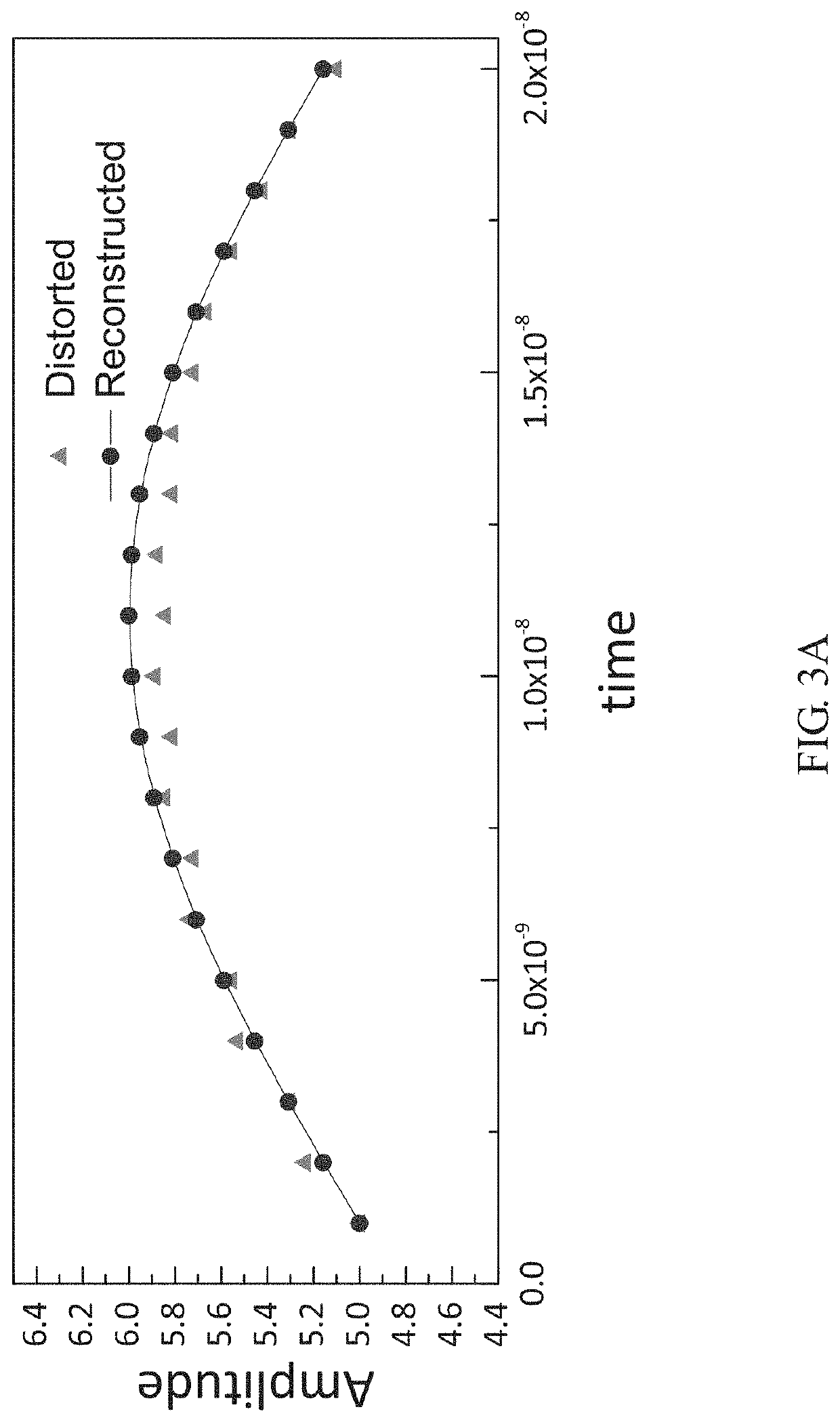
High-speed and high-precision photonic analog-to-digital conversion device and method for realizing intelligent signal processing using the same
PatentActiveUS10651867B2
Innovation
- Integration of deep learning technology into the photonic analog-to-digital conversion system, utilizing a high-speed photonic analog-to-digital conversion device with a deep learning signal processing module that learns and corrects nonlinear responses and channel mismatches, enabling intelligent signal processing.
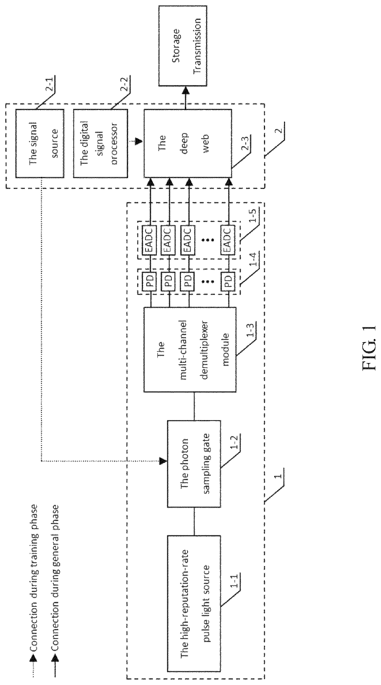

Method and system for intelligent decision-making photonic signal processing
PatentActiveUS11526742B2
Innovation
- An intelligent decision-making photonic signal processing system combining photonic technology with deep learning, utilizing a multi-functional input unit, electro-optical conversion module, signal processing module, photoelectric conversion module, and an artificial intelligence chip to enable simultaneous digital and analog signal processing, leveraging heterogeneous photoelectron hybrid integration and packaging for real-time processing.


Energy Efficiency Standards for Photonic Computing Systems
Energy efficiency has emerged as a critical performance metric for photonic computing systems designed to accelerate high-speed AI models. As these systems process massive datasets and complex neural network operations, establishing comprehensive energy efficiency standards becomes essential for sustainable deployment and commercial viability. Current industry initiatives focus on developing standardized measurement protocols that account for the unique characteristics of photonic signal processing architectures.
The IEEE and International Electrotechnical Commission have begun preliminary work on defining energy efficiency benchmarks specifically tailored for photonic AI accelerators. These standards consider factors such as optical power consumption, thermal management requirements, and the energy overhead associated with electro-optical conversions. Unlike traditional electronic systems, photonic processors exhibit non-linear energy scaling behaviors that necessitate specialized evaluation methodologies.
Key performance indicators under development include photons-per-operation metrics, optical signal-to-noise ratio efficiency, and wavelength utilization effectiveness. These metrics aim to capture the fundamental energy characteristics of photonic matrix multiplication, convolution operations, and activation functions commonly used in AI workloads. The standards also address energy measurement across different operational modes, including training and inference phases.
Thermal efficiency standards represent another crucial component, as photonic systems generate heat through laser sources, modulators, and photodetectors. Proposed guidelines establish maximum thermal design power limits and cooling efficiency requirements to ensure optimal performance while minimizing energy waste. These standards also incorporate ambient temperature considerations and thermal cycling effects on long-term energy performance.
Emerging standards frameworks emphasize the importance of system-level energy accounting, including peripheral components such as electronic control circuits, memory interfaces, and optical switching networks. This holistic approach ensures that energy efficiency measurements reflect real-world deployment scenarios rather than isolated component performance. The standards also define testing conditions, measurement precision requirements, and certification procedures for commercial photonic AI systems.
Integration Challenges of Photonic-Electronic Hybrid Systems
The integration of photonic and electronic components in high-speed AI processing systems presents multifaceted challenges that span material science, manufacturing precision, and system architecture design. The fundamental mismatch between photonic and electronic operating principles creates inherent difficulties in achieving seamless signal conversion and maintaining data integrity across hybrid interfaces.
Material compatibility represents a primary obstacle in photonic-electronic integration. Silicon photonics platforms, while offering CMOS compatibility, exhibit limitations in direct bandgap properties essential for efficient light emission. III-V semiconductor materials provide superior optical characteristics but require complex heterogeneous integration processes with silicon electronics. The thermal expansion coefficient differences between these materials introduce mechanical stress during fabrication and operation, potentially degrading device performance and reliability.
Manufacturing precision requirements pose significant scalability challenges. Photonic components demand nanometer-level alignment tolerances for efficient optical coupling, while electronic circuits require precise doping profiles and metallization patterns. The integration process must accommodate both requirements simultaneously, leading to increased fabrication complexity and reduced yield rates. Advanced packaging techniques, including flip-chip bonding and through-silicon vias, are necessary but add substantial cost and manufacturing complexity.
Signal conversion efficiency between optical and electrical domains remains a critical bottleneck. Photodetectors and modulators introduce latency and power consumption that can offset the speed advantages of photonic processing. The conversion process also introduces noise and signal degradation, particularly challenging for AI applications requiring high precision arithmetic operations. Maintaining signal-to-noise ratios across multiple conversion stages requires sophisticated error correction and signal conditioning circuits.
Thermal management in hybrid systems presents unique challenges due to the different thermal sensitivities of photonic and electronic components. Laser sources and modulators exhibit temperature-dependent wavelength drift, while electronic circuits generate localized heat that affects nearby photonic elements. Effective thermal isolation and active cooling systems are essential but increase system complexity and power consumption, potentially undermining the energy efficiency benefits of photonic processing.
Unlock deeper insights with PatSnap Eureka Quick Research — get a full tech report to explore trends and direct your research. Try now!
Generate Your Research Report Instantly with AI Agent
Supercharge your innovation with PatSnap Eureka AI Agent Platform!