Photonics Interposers for Cloud Computing: Latency Reduction
APR 15, 20269 MIN READ
Generate Your Research Report Instantly with AI Agent
Patsnap Eureka helps you evaluate technical feasibility & market potential.
Photonic Interposer Technology Background and Objectives
Photonic interposer technology represents a revolutionary approach to addressing the escalating latency challenges in modern cloud computing infrastructure. As data centers continue to scale and computational demands intensify, traditional electronic interconnects have reached fundamental physical limitations in terms of bandwidth density and signal propagation speed. The emergence of photonic interposers offers a paradigm shift by leveraging optical signal transmission to overcome these constraints, enabling unprecedented data transfer rates while significantly reducing latency penalties that plague current electronic systems.
The historical evolution of photonic integration began in the 1980s with basic optical waveguide structures, progressing through silicon photonics development in the 2000s, and culminating in today's sophisticated photonic interposer platforms. This technological trajectory has been driven by the relentless pursuit of higher bandwidth, lower power consumption, and reduced form factors in data communication systems. The convergence of mature semiconductor fabrication processes with advanced optical design principles has created the foundation for practical photonic interposer implementations.
Current cloud computing architectures face critical bottlenecks in inter-processor communication, memory access, and rack-to-rack connectivity, where electronic signals experience significant propagation delays and bandwidth limitations. These constraints directly impact application performance, particularly in latency-sensitive workloads such as real-time analytics, high-frequency trading, and interactive services. The speed of light advantage inherent in optical transmission, combined with the ability to multiplex multiple wavelengths simultaneously, positions photonic interposers as a transformative solution.
The primary technical objectives driving photonic interposer development include achieving sub-nanosecond latency for short-reach communications, enabling terabit-scale aggregate bandwidth within compact form factors, and maintaining energy efficiency comparable to or superior than electronic alternatives. Additionally, seamless integration with existing electronic processing units and cost-effective manufacturing scalability represent crucial implementation goals.
Advanced photonic interposer designs incorporate sophisticated components including high-speed modulators, low-loss waveguides, wavelength division multiplexing capabilities, and integrated photodetectors. These elements work synergistically to create optical pathways that bypass traditional electronic routing limitations, enabling direct optical connections between processing elements with minimal latency overhead and maximum bandwidth utilization efficiency.
Cloud Computing Market Demand for Low-Latency Solutions
The cloud computing industry faces unprecedented pressure to minimize latency as digital transformation accelerates across enterprises worldwide. Modern applications including real-time analytics, artificial intelligence workloads, and high-frequency trading systems demand ultra-low latency communication between distributed computing resources. Traditional electrical interconnects in data centers have reached fundamental physical limitations, creating bottlenecks that constrain overall system performance and user experience.
Financial services organizations require microsecond-level response times for algorithmic trading platforms, where even nanosecond delays can result in significant revenue losses. Similarly, autonomous vehicle systems processing real-time sensor data through cloud infrastructure cannot tolerate communication delays that might compromise safety-critical decision making. These stringent requirements drive substantial market demand for breakthrough interconnect technologies.
Edge computing deployments further intensify latency requirements as processing moves closer to end users. Content delivery networks, gaming platforms, and augmented reality applications depend on seamless data flow between edge nodes and central cloud resources. Current copper-based and traditional optical solutions struggle to meet the combined demands of bandwidth density and latency reduction required by these emerging use cases.
Hyperscale cloud providers actively seek solutions that can reduce inter-rack and intra-rack communication delays while maintaining cost efficiency at massive scale. The proliferation of containerized applications and microservices architectures creates additional complexity, as these distributed systems generate numerous small data packets requiring rapid processing and routing. Network congestion and queuing delays in traditional switching infrastructure compound these challenges.
Machine learning inference workloads represent another critical driver, as model serving requires rapid data movement between memory, processing units, and storage systems. Large language models and computer vision applications processing streaming data cannot afford communication bottlenecks that would degrade real-time performance expectations. The market increasingly recognizes that photonic solutions offer fundamental advantages over electrical alternatives in addressing these latency-sensitive applications.
Enterprise customers demonstrate willingness to invest in premium interconnect technologies that deliver measurable performance improvements, particularly when these solutions enable new revenue opportunities or competitive advantages in their respective markets.
Current State and Challenges of Photonic Integration
Photonic integration technology has reached a critical juncture where significant progress coexists with substantial technical barriers. Current silicon photonics platforms demonstrate mature capabilities in basic optical components, including waveguides, modulators, and photodetectors. Leading foundries such as GlobalFoundries, TSMC, and Intel have established production-ready processes that enable integration of photonic devices with CMOS electronics on the same substrate.
The state-of-the-art photonic interposers currently achieve data transmission rates exceeding 100 Gbps per channel, with some experimental demonstrations reaching terabit-scale aggregate bandwidth. These systems typically operate at wavelengths around 1310 nm and 1550 nm, leveraging wavelength division multiplexing to maximize throughput. Commercial solutions from companies like Ayar Labs and Lightmatter have demonstrated functional prototypes connecting processors and memory systems with sub-nanosecond latencies.
However, several fundamental challenges continue to impede widespread adoption in cloud computing environments. Optical loss remains a primary concern, with typical silicon photonic circuits experiencing 0.1-0.5 dB/cm propagation losses and coupling losses of 1-3 dB at fiber interfaces. These losses accumulate across complex routing paths, necessitating optical amplification that introduces noise and power consumption penalties.
Thermal management presents another significant obstacle. Photonic devices exhibit strong temperature sensitivity, with wavelength drift rates of approximately 0.1 nm/°C for silicon ring resonators. This sensitivity requires active thermal control systems that consume additional power and increase system complexity, potentially offsetting the energy efficiency advantages of optical interconnects.
Manufacturing yield and reliability issues further complicate deployment scenarios. Process variations in silicon photonics fabrication can cause wavelength mismatches between devices, requiring extensive post-fabrication tuning or trimming procedures. The long-term reliability of integrated photonic components under continuous operation remains less established compared to mature electronic systems.
Integration complexity at the system level poses additional challenges. Current photonic interposers require sophisticated control electronics for wavelength stabilization, power management, and signal conditioning. The interface between optical and electrical domains introduces latency penalties and power conversion inefficiencies that can diminish overall system performance gains.
Packaging and assembly represent critical bottlenecks in achieving cost-effective solutions. Precise optical alignment requirements during assembly demand specialized equipment and processes, significantly increasing manufacturing costs compared to purely electronic solutions. The development of standardized packaging approaches remains an ongoing industry challenge that affects scalability prospects.
Existing Photonic Interposer Solutions
01 Optical interconnect structures for reduced signal propagation delay
Photonic interposers utilize optical waveguides and interconnects to transmit signals between components, significantly reducing latency compared to traditional electrical interconnects. These structures employ optical pathways that enable high-speed data transmission with minimal signal degradation. The integration of optical components directly into the interposer substrate allows for shorter signal paths and faster communication between chips and modules.- Optical interconnect structures for reduced signal propagation delay: Photonic interposers utilize optical waveguides and interconnect structures to minimize signal latency compared to traditional electrical interconnects. These structures enable direct optical signal transmission between chips or components, significantly reducing propagation delays. The optical pathways are designed with optimized geometries and materials to achieve minimal signal distortion and maximum transmission speed.
- Integration of optical and electrical layers for latency optimization: Hybrid interposer designs combine optical transmission layers with electrical routing layers to balance performance and functionality. The optical layer handles high-speed data transmission with minimal latency, while the electrical layer manages control signals and power distribution. This integration approach allows for optimized signal routing paths that minimize overall system latency while maintaining compatibility with existing electronic components.
- Wavelength division multiplexing for parallel data transmission: Multiple wavelengths are utilized simultaneously through the same optical pathway to increase data throughput without increasing latency. This technique allows parallel transmission of multiple data streams, effectively reducing the time required for data transfer. The interposer incorporates wavelength-selective components and multiplexing structures to manage different optical channels efficiently.
- Short-distance optical coupling mechanisms: Direct optical coupling techniques are employed to minimize the physical distance signals must travel between components. These mechanisms include vertical cavity surface emitting lasers, micro-lenses, and direct-bonded optical interfaces that reduce signal path length. By minimizing the physical transmission distance, these coupling approaches directly reduce propagation latency in photonic interposer systems.
- Low-loss optical materials and waveguide designs: Advanced materials with minimal optical absorption and scattering properties are utilized to reduce signal attenuation and maintain signal integrity. Waveguide structures are designed with optimized cross-sectional profiles and bend radii to minimize modal dispersion and propagation losses. These design considerations ensure that signals maintain their quality and timing characteristics throughout transmission, contributing to overall latency reduction.
02 Three-dimensional photonic integration for minimizing transmission distance
Three-dimensional integration techniques stack multiple photonic and electronic layers within the interposer to minimize the physical distance signals must travel. This vertical integration approach reduces latency by creating direct optical paths between components at different layers. The architecture enables compact packaging while maintaining high bandwidth and low latency characteristics essential for high-performance computing applications.Expand Specific Solutions03 Wavelength division multiplexing for parallel data transmission
Wavelength division multiplexing technology enables multiple data channels to be transmitted simultaneously through a single optical waveguide by using different wavelengths of light. This parallel transmission capability significantly increases bandwidth while maintaining low latency. The technique allows for efficient use of the photonic interposer's optical infrastructure and reduces the need for multiple physical connections.Expand Specific Solutions04 Hybrid electrical-optical routing for optimized signal paths
Hybrid interposer designs combine electrical and optical routing to optimize signal transmission based on distance and bandwidth requirements. Short-distance connections may use electrical paths while longer connections utilize optical channels to minimize overall latency. This approach provides flexibility in system design and allows for efficient resource allocation based on specific performance requirements.Expand Specific Solutions05 Advanced packaging techniques for reduced coupling losses
Specialized packaging and alignment techniques minimize optical coupling losses between photonic components and waveguides within the interposer. Precise alignment mechanisms and optimized coupling structures ensure efficient light transmission with minimal signal loss. These techniques reduce the need for signal amplification and associated delays, contributing to overall latency reduction in photonic interposer systems.Expand Specific Solutions
Key Players in Photonic Computing Industry
The photonics interposers market for cloud computing latency reduction is in an emerging growth phase, driven by increasing demand for high-speed data processing and reduced latency in cloud infrastructure. The market shows significant potential with early-stage commercial deployments, though still developing toward mainstream adoption. Technology maturity varies considerably across players, with specialized photonics companies like Lightmatter and PsiQuantum leading innovation in photonic computing solutions, while established tech giants including Samsung Electronics, IBM, and Huawei leverage their manufacturing capabilities and market presence to integrate photonic technologies. Infrastructure providers such as Hewlett Packard Enterprise focus on system-level integration, while foundries like Advanced Micro Foundry and Soitec provide critical manufacturing capabilities. The competitive landscape reflects a convergence of pure-play photonics innovators, semiconductor incumbents, and cloud infrastructure providers, indicating the technology's transition from research to commercial viability.
Lightmatter, Inc.
Technical Solution: Lightmatter develops photonic interconnect solutions that utilize silicon photonics technology to create high-bandwidth, low-latency connections for data centers and cloud computing infrastructure. Their photonic interposer technology integrates optical waveguides directly into silicon substrates, enabling light-based data transmission that significantly reduces signal propagation delays compared to traditional electrical interconnects. The company's approach focuses on creating photonic fabric architectures that can handle massive parallel data flows with sub-microsecond latencies, specifically designed for AI workloads and high-performance computing applications in cloud environments.
Strengths: Native photonic interconnect expertise, purpose-built for cloud computing latency reduction. Weaknesses: Limited manufacturing scale and higher initial deployment costs compared to established electrical solutions.
Huawei Technologies Co., Ltd.
Technical Solution: Huawei has developed comprehensive photonic interposer solutions as part of their optical networking portfolio for cloud infrastructure. Their technology integrates silicon photonic components with advanced packaging techniques to create high-density optical interconnects that reduce data transmission latency in cloud data centers. The company's photonic interposer designs incorporate wavelength division multiplexing (WDM) capabilities and advanced modulation formats to achieve high bandwidth density while maintaining low power consumption. Their solutions target hyperscale data center applications where minimizing east-west traffic latency is critical for distributed computing performance.
Strengths: Extensive R&D resources, integrated hardware-software optimization, strong manufacturing capabilities. Weaknesses: Geopolitical restrictions may limit market access in certain regions, dependency on external silicon photonics foundries.
Core Innovations in Photonic Latency Reduction
Electrical and optical interconnect links combined in a hybrid interposer
PatentWO2025217567A1
Innovation
- A hybrid photonic-electric interposer with parallel electrical and photonic signal paths, where photonic parts include light emitting devices and waveguides, allowing direct connections between any points on dies within a package, using low-power, incoherent optical signals for long distances and synchronous communication.


Method And System For A Photonic Interposer
PatentActiveUS20120177381A1
Innovation
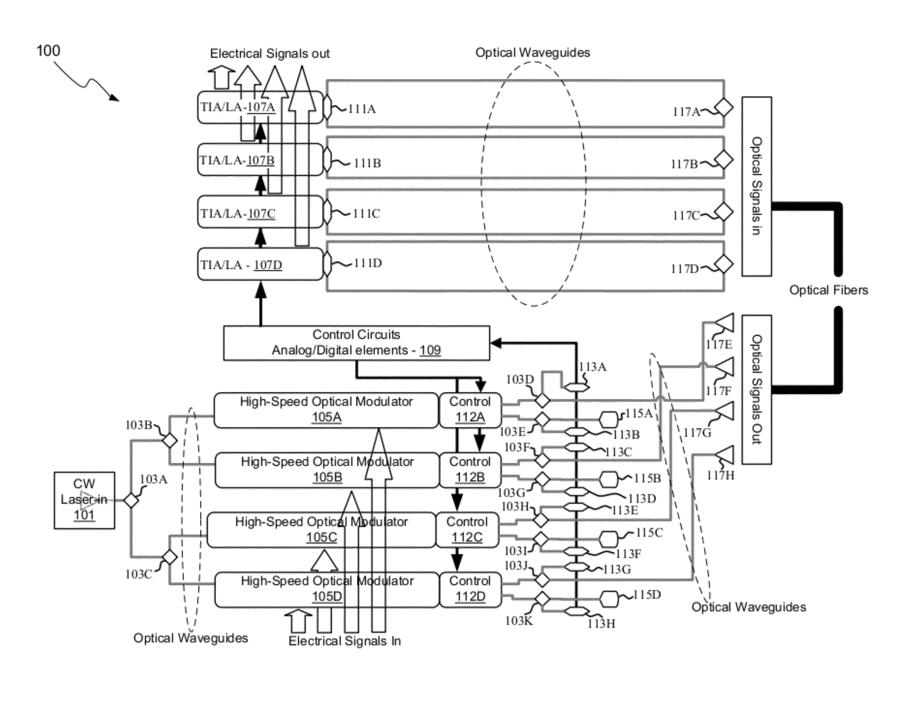
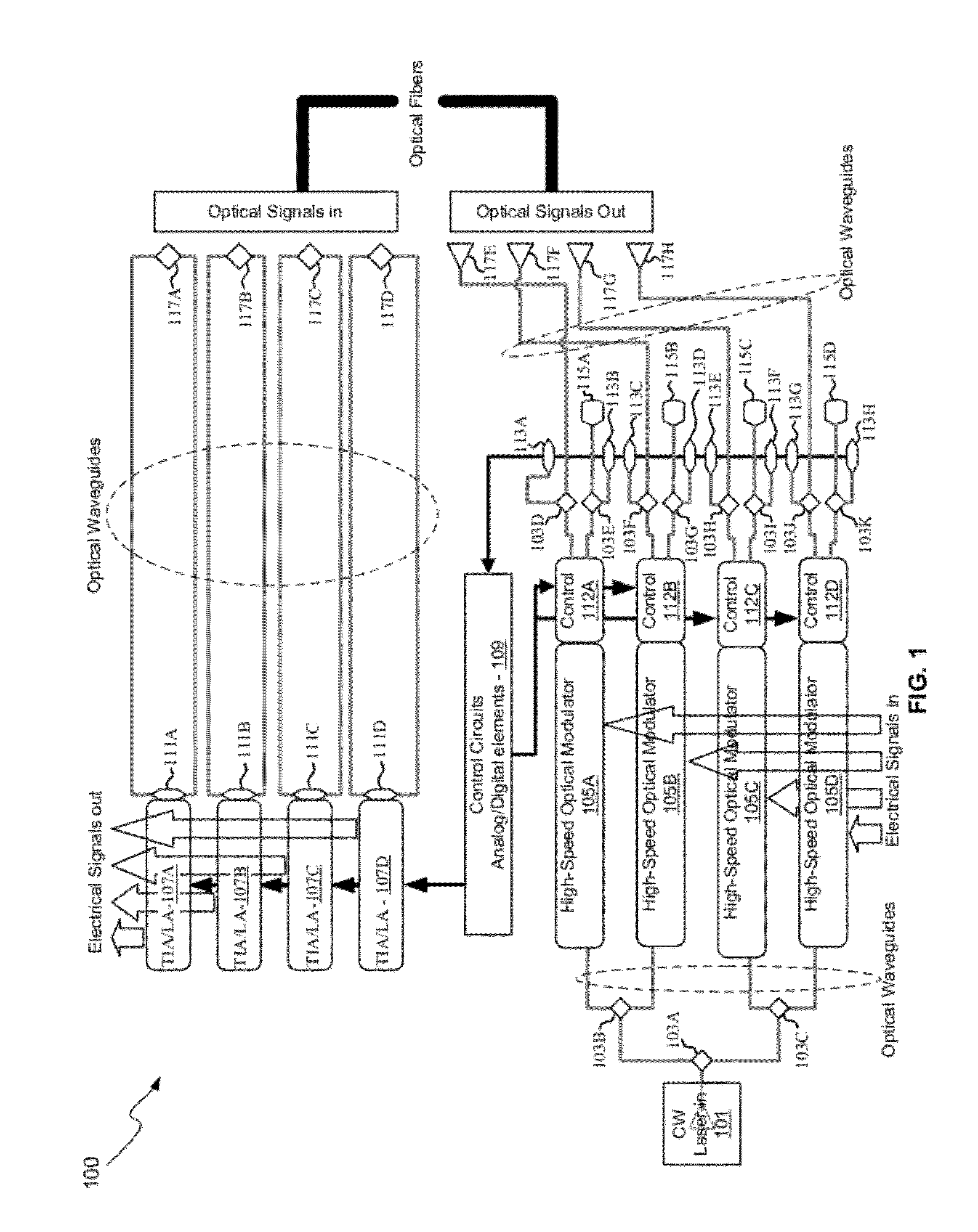
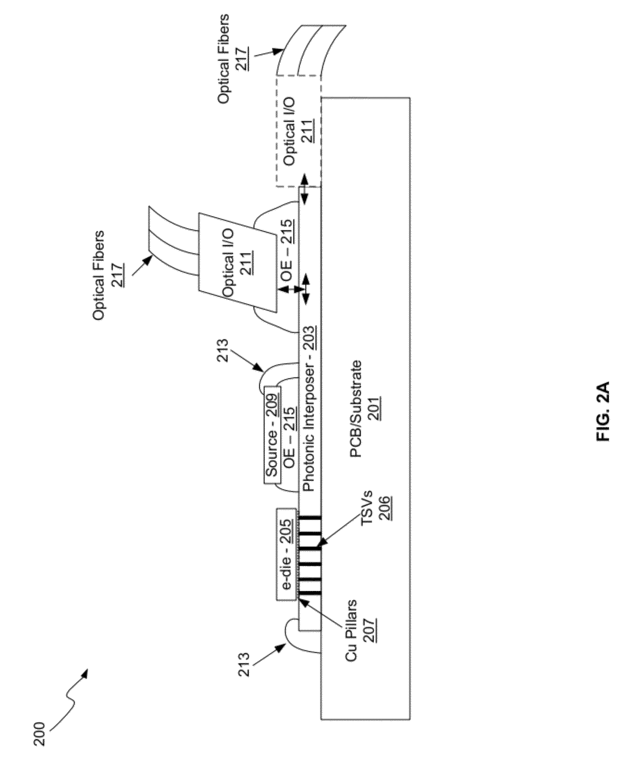
- A photonic interposer system that integrates silicon photonic devices with CMOS electronics, using Mach-Zehnder interferometer modulators, photodetectors, and grating couplers to process and transmit continuous-wave optical signals, enabling high-speed communication through optical waveguides and copper pillars, allowing independent optimization of electronic and photonic performance.

Standardization Framework for Photonic Interposers
The standardization framework for photonic interposers represents a critical infrastructure requirement for enabling widespread adoption of photonic integration technologies in cloud computing environments. Current standardization efforts are fragmented across multiple organizations, including IEEE, ITU-T, and OIF, each addressing different aspects of photonic integration without comprehensive coordination. This fragmentation creates significant barriers to interoperability and scalability in cloud data center deployments.
The IEEE 802.3 working group has established preliminary guidelines for optical interconnects, while the ITU-T Study Group 15 focuses on optical transport network standards. However, these existing frameworks primarily address fiber-optic communications rather than the specific requirements of photonic interposers for silicon photonics integration. The lack of unified standards for mechanical interfaces, electrical connectivity, and thermal management creates compatibility challenges across different vendor solutions.
A comprehensive standardization framework must address multiple technical domains simultaneously. Physical layer specifications require standardized dimensions, pin configurations, and mounting mechanisms to ensure mechanical compatibility across different platforms. Electrical interface standards must define power delivery, signal integrity requirements, and electromagnetic compatibility guidelines. Optical interface specifications need to establish connector types, wavelength allocations, and power budgets for consistent performance across vendors.
Protocol standardization presents additional complexity, particularly regarding control plane interfaces and management protocols. The framework must define standardized APIs for photonic device configuration, monitoring, and fault management. This includes establishing common data models for photonic component characteristics and performance metrics that enable seamless integration with existing cloud infrastructure management systems.
Testing and certification procedures form another essential component of the standardization framework. Standardized test methodologies must be established for evaluating latency performance, power consumption, thermal characteristics, and reliability metrics. These procedures should include both component-level testing protocols and system-level integration validation requirements to ensure consistent performance across different deployment scenarios.
The framework must also address manufacturing standards to enable cost-effective mass production. This includes standardized fabrication processes, quality control procedures, and supply chain requirements that support the scalability demands of cloud computing infrastructure. Establishing these manufacturing standards will facilitate vendor ecosystem development and drive down costs through economies of scale.
Thermal Management in High-Density Photonic Systems
Thermal management represents one of the most critical engineering challenges in high-density photonic systems designed for cloud computing applications. As photonic interposers integrate increasing numbers of optical components within confined spaces to achieve ultra-low latency performance, the resulting heat generation and dissipation requirements become exponentially more complex. The concentrated power density in these systems can reach levels exceeding 1000 W/cm², creating thermal hotspots that significantly impact system reliability and performance.
The fundamental challenge stems from the inherent sensitivity of photonic components to temperature variations. Laser diodes, modulators, and photodetectors exhibit wavelength drift, efficiency degradation, and reliability issues when operating outside optimal temperature ranges. In silicon photonic systems, temperature coefficients can cause wavelength shifts of approximately 0.1 nm/°C, which directly affects signal integrity and system performance in wavelength-division multiplexing applications.
Advanced thermal management strategies for high-density photonic interposers encompass multiple approaches operating at different scales. Micro-scale solutions include integrated thermal interface materials with enhanced conductivity, such as graphene-based composites and carbon nanotube arrays, which provide efficient heat transfer pathways from individual components to heat spreaders. These materials can achieve thermal conductivities exceeding 1000 W/m·K while maintaining electrical isolation.
Macro-scale thermal management involves sophisticated cooling architectures including liquid cooling systems with microfluidic channels embedded within the interposer substrate. These systems utilize specialized coolants with optimized thermal properties and flow characteristics to maintain uniform temperature distribution across the photonic array. Advanced implementations incorporate closed-loop temperature control with real-time monitoring and adaptive cooling strategies.
Emerging thermal management technologies focus on active cooling integration directly within the photonic substrate. Thermoelectric coolers and micro-refrigeration systems enable localized temperature control for critical components, while thermal spreaders with engineered metamaterial structures provide enhanced heat distribution capabilities. Additionally, advanced packaging techniques utilizing multi-layer thermal architectures and phase-change materials offer promising solutions for transient thermal management during peak computational loads.
The integration of thermal management systems must carefully balance cooling efficiency with optical performance requirements, ensuring that thermal solutions do not introduce optical losses, mechanical stress, or electromagnetic interference that could compromise the primary latency reduction objectives of photonic interposer systems.
Unlock deeper insights with Patsnap Eureka Quick Research — get a full tech report to explore trends and direct your research. Try now!
Generate Your Research Report Instantly with AI Agent
Supercharge your innovation with Patsnap Eureka AI Agent Platform!