Photonics Interposers' Impact on Network Latency Evaluations
APR 15, 20269 MIN READ
Generate Your Research Report Instantly with AI Agent
Patsnap Eureka helps you evaluate technical feasibility & market potential.
Photonic Interposer Technology Background and Objectives
Photonic interposer technology represents a paradigm shift in high-performance computing and data center architectures, emerging from the convergence of silicon photonics and advanced packaging solutions. This technology addresses the fundamental bottleneck of electrical interconnects in modern computing systems, where traditional copper-based connections increasingly limit performance due to signal integrity issues, power consumption, and bandwidth constraints at high frequencies.
The historical development of photonic interposers traces back to the early 2000s when researchers began exploring silicon photonics as a viable alternative to electronic interconnects. Initial efforts focused on integrating optical components with electronic circuits on silicon substrates, leveraging existing semiconductor manufacturing processes. The technology gained significant momentum around 2010 when major semiconductor companies recognized the potential for optical interconnects to overcome the limitations of Moore's Law scaling.
Current technological evolution demonstrates a clear trajectory toward higher integration density and improved performance metrics. Modern photonic interposers incorporate wavelength division multiplexing, advanced modulation formats, and sophisticated packaging techniques that enable unprecedented data transmission rates while maintaining compatibility with existing electronic systems. The technology has progressed from laboratory demonstrations to commercial implementations in high-end data center applications.
The primary objective of photonic interposer technology centers on dramatically reducing network latency while simultaneously increasing bandwidth capacity. Traditional electrical interconnects introduce significant propagation delays, especially in multi-hop network configurations where signals must traverse multiple switching layers. Photonic interposers aim to eliminate these bottlenecks by providing direct optical pathways between processing elements, potentially reducing latency by orders of magnitude.
Performance targets for next-generation photonic interposers include achieving sub-nanosecond latency for chip-to-chip communications, supporting aggregate bandwidths exceeding multiple terabits per second, and maintaining energy efficiency below 1 picojoule per bit. These objectives directly address the growing demands of artificial intelligence workloads, high-frequency trading systems, and real-time data processing applications where latency optimization is critical.
The strategic importance of photonic interposers extends beyond immediate performance improvements to encompass fundamental architectural transformations in computing systems. By enabling efficient optical interconnects at the package level, this technology facilitates new system designs that can scale beyond traditional electrical limitations, supporting the continued advancement of high-performance computing platforms and next-generation network infrastructures.
Market Demand for Low-Latency Network Solutions
The telecommunications and data center industries are experiencing unprecedented demand for ultra-low latency network solutions, driven by the explosive growth of real-time applications and latency-sensitive workloads. High-frequency trading platforms, autonomous vehicle communications, augmented reality applications, and industrial IoT systems require network latencies measured in microseconds rather than milliseconds. This stringent requirement has created a substantial market opportunity for advanced networking technologies that can minimize signal propagation delays and processing overhead.
Cloud service providers and hyperscale data centers represent the largest segment of demand for low-latency solutions. These organizations are investing heavily in infrastructure upgrades to support emerging applications such as edge computing, real-time analytics, and distributed artificial intelligence workloads. The proliferation of 5G networks has further intensified the need for ultra-low latency backhaul and fronthaul connections, as network operators strive to meet the sub-millisecond latency requirements promised by next-generation wireless standards.
Financial services institutions constitute another critical market segment driving demand for low-latency networking solutions. Algorithmic trading systems and high-frequency trading operations depend on microsecond-level advantages to maintain competitive positioning. These organizations are willing to invest significantly in specialized networking infrastructure that can provide even marginal latency improvements, creating a premium market for advanced photonic interconnect technologies.
The gaming and entertainment industry has emerged as a rapidly growing market for low-latency solutions. Online gaming platforms, virtual reality experiences, and interactive streaming services require consistent, predictable network performance to deliver acceptable user experiences. The shift toward cloud-based gaming and remote rendering applications has amplified the importance of minimizing network-induced delays throughout the entire data path.
Enterprise applications are increasingly demanding lower network latencies as organizations adopt real-time collaboration tools, distributed computing architectures, and time-sensitive industrial control systems. Manufacturing facilities implementing Industry 4.0 initiatives require deterministic network performance for robotic control systems and synchronized production processes. These applications cannot tolerate the variable latencies associated with traditional networking approaches, creating sustained demand for specialized low-latency infrastructure solutions.
Market research indicates that organizations are prioritizing network latency reduction as a key performance metric, often ranking it above traditional considerations such as bandwidth capacity or cost optimization. This shift in priorities reflects the growing recognition that application performance and user experience are directly correlated with end-to-end network latency characteristics.
Current State of Photonic Integration and Latency Challenges
Photonic integration technology has reached a critical juncture where silicon photonics platforms demonstrate mature fabrication capabilities, yet significant latency challenges persist in high-performance computing and telecommunications applications. Current photonic interposers leverage advanced silicon-on-insulator (SOI) and indium phosphide (InP) platforms to achieve optical-electrical-optical conversions, but these implementations introduce measurable latency penalties that impact network performance evaluations.
The state-of-the-art photonic integration primarily relies on wavelength division multiplexing (WDM) architectures integrated with electronic switching fabrics. Leading foundries such as GlobalFoundries, TSMC, and specialized facilities like AIM Photonics have established process design kits supporting multi-project wafer runs, enabling standardized photonic component libraries. However, these platforms exhibit inherent latency characteristics ranging from 50 to 200 nanoseconds per optical hop, significantly impacting time-sensitive applications.
Current latency challenges stem from multiple sources within photonic interposer architectures. Optical-to-electrical conversion processes introduce fundamental delays through photodetector response times and transimpedance amplifier settling periods. Electronic packet processing and routing decisions within the interposer add additional microsecond-scale delays, while optical switching elements such as Mach-Zehnder modulators and ring resonators contribute phase-dependent latency variations.
Thermal management represents another critical challenge affecting latency consistency in photonic systems. Temperature fluctuations cause wavelength drift in silicon photonic devices, necessitating active thermal control mechanisms that introduce feedback loop delays. These thermal effects create dynamic latency variations that complicate network timing protocols and quality-of-service guarantees.
Manufacturing variability across photonic wafers creates device-to-device performance disparities that manifest as latency distribution spreads. Process variations in waveguide dimensions, doping concentrations, and coupling efficiencies result in non-uniform propagation delays across identical circuit designs. This variability challenges system-level timing closure and requires sophisticated calibration mechanisms.
Integration density limitations currently constrain the co-location of optical and electronic functions, forcing designers to implement longer electrical interconnects between photonic and CMOS sections. These extended routing paths contribute additional propagation delays and signal integrity challenges that compound overall system latency.
The geographic distribution of photonic integration capabilities remains concentrated in established semiconductor manufacturing regions, with limited access to specialized fabrication processes creating supply chain dependencies that affect development timelines and cost structures for latency-optimized designs.
Current Photonic Interposer Solutions for Latency Reduction
01 Photonic interposer architecture for reduced signal propagation delay
Photonic interposers utilize optical waveguides and photonic integrated circuits to transmit data signals between components, significantly reducing propagation delays compared to traditional electrical interconnects. The architecture incorporates optical routing structures that enable high-speed data transmission with minimal latency by leveraging the speed of light for signal propagation across the interposer substrate.- Photonic interposer architecture for reduced signal propagation delay: Photonic interposers utilize optical waveguides and photonic integrated circuits to transmit data signals between chips or components. By replacing traditional electrical interconnects with optical pathways, signal propagation occurs at the speed of light in the medium, significantly reducing latency. The architecture includes optical coupling structures, waveguide routing, and photodetectors that enable high-speed data transfer with minimal delay compared to conventional electrical interposers.
- Optical switching and routing mechanisms for low-latency networks: Advanced optical switching technologies integrated into photonic interposers enable dynamic routing of optical signals with minimal latency. These mechanisms include optical crossbar switches, wavelength-selective switches, and fast reconfigurable optical paths that eliminate the need for optical-electrical-optical conversion. The switching architectures support high-bandwidth communication while maintaining nanosecond-scale switching times, thereby reducing overall network latency in data center and high-performance computing applications.
- Wavelength division multiplexing for parallel data transmission: Wavelength division multiplexing techniques implemented in photonic interposers allow multiple data channels to be transmitted simultaneously over the same optical waveguide using different wavelengths. This parallel transmission capability dramatically increases aggregate bandwidth while maintaining low latency for individual channels. The technology includes wavelength multiplexers, demultiplexers, and multi-wavelength laser sources that enable efficient utilization of optical bandwidth without introducing significant signal delay.
- Integration of optical transceivers with minimal conversion latency: Photonic interposers incorporate closely integrated optical transceivers that minimize the latency associated with electrical-to-optical and optical-to-electrical signal conversion. These transceivers feature high-speed modulators, photodetectors, and driver circuits positioned in close proximity to reduce parasitic effects and signal path lengths. The integration approach reduces conversion delays to picosecond ranges, enabling ultra-low-latency communication between electronic processing units and optical networks.
- Thermal management and signal integrity optimization: Effective thermal management solutions in photonic interposers prevent temperature-induced variations in optical signal propagation that could increase latency. These solutions include integrated thermal sensors, heat dissipation structures, and temperature-stabilized optical components that maintain consistent signal transmission characteristics. Additionally, signal integrity optimization techniques such as dispersion compensation and noise reduction ensure that optical signals maintain their quality over transmission paths, preventing retransmission delays and maintaining predictable low-latency performance.
02 Optical switching and routing mechanisms for latency optimization
Advanced optical switching technologies integrated within photonic interposers enable dynamic routing of optical signals with minimal switching delays. These mechanisms employ fast optical switches and crossbar architectures that allow for reconfigurable data paths, reducing network congestion and optimizing signal routing to minimize end-to-end latency in multi-chip photonic systems.Expand Specific Solutions03 Wavelength division multiplexing for parallel data transmission
Wavelength division multiplexing techniques are employed in photonic interposers to enable simultaneous transmission of multiple data channels over the same optical waveguide using different wavelengths. This parallel transmission capability significantly increases bandwidth utilization and reduces latency by allowing concurrent data transfers without channel interference or queuing delays.Expand Specific Solutions04 Integration of optical transceivers with minimal conversion latency
Photonic interposers incorporate closely integrated optical transceivers that perform electro-optical and opto-electrical conversions with optimized designs to minimize conversion latency. The transceivers are positioned strategically on the interposer to reduce signal path lengths and employ high-speed modulation techniques that enable rapid signal conversion between electrical and optical domains.Expand Specific Solutions05 Thermal management and signal integrity for consistent low-latency performance
Effective thermal management solutions integrated into photonic interposers maintain stable operating temperatures, ensuring consistent signal propagation speeds and preventing thermal-induced latency variations. The designs incorporate heat dissipation structures and temperature monitoring systems that preserve signal integrity and maintain predictable low-latency performance across varying operational conditions.Expand Specific Solutions
Key Players in Photonic Interposer and Network Industry
The photonics interposers market for network latency applications is in an emerging growth stage, driven by increasing demand for high-speed data processing and reduced latency in AI, telecommunications, and data center applications. The market shows significant potential with a diverse competitive landscape spanning established semiconductor giants and specialized photonics innovators. Technology maturity varies considerably across players: industry leaders like Intel, Huawei, and Cisco leverage extensive R&D capabilities and manufacturing scale, while specialized companies such as Lightmatter, HyperLight Corp., and PsiQuantum focus on cutting-edge photonic solutions. Academic institutions including MIT, Columbia University, and National University of Singapore contribute foundational research, accelerating innovation. The sector demonstrates strong momentum with companies like Shanghai Xizhi Technology and established players like Corning providing critical infrastructure components, indicating a maturing ecosystem poised for substantial market expansion.
Lightmatter, Inc.
Technical Solution: Lightmatter develops photonic interconnect solutions that utilize silicon photonics technology to create high-bandwidth, low-latency communication pathways between processors and memory systems. Their photonic interposer technology enables direct optical connections that can achieve sub-nanosecond latency improvements compared to traditional electrical interconnects. The company's approach integrates photonic waveguides directly into the interposer substrate, allowing for parallel data transmission at wavelengths around 1310nm and 1550nm. This architecture supports bandwidth densities exceeding 1Tbps per square millimeter while maintaining power efficiency below 1pJ per bit for short-reach communications.
Strengths: Pioneering commercial photonic interconnect solutions with proven latency reduction capabilities and high bandwidth density. Weaknesses: Limited to short-reach applications and requires specialized manufacturing processes that increase production costs.
Huawei Technologies Co., Ltd.
Technical Solution: Huawei has developed advanced photonic interposer technologies for data center and telecommunications applications, focusing on reducing network latency through integrated silicon photonics solutions. Their approach combines electronic and photonic components on a single interposer platform, enabling high-speed optical signal processing with latencies reduced by up to 40% compared to conventional electronic switching. The technology incorporates wavelength division multiplexing (WDM) capabilities supporting up to 64 channels per fiber, with each channel operating at 25Gbps or higher. Huawei's photonic interposers are designed for scalable deployment in 5G networks and cloud computing infrastructures where microsecond-level latency improvements are critical.
Strengths: Comprehensive integration capabilities with strong R&D resources and proven deployment in telecommunications infrastructure. Weaknesses: Geopolitical restrictions may limit market access and technology sharing in certain regions.
Core Patents in Photonic Interposer Latency Optimization
Photonic communication platform and related architectures, systems and methods
PatentPendingUS20250337504A1
Innovation
- The use of photonic interposers with programmable photonic tiles and optical connections, enabling low-power, high-bandwidth communication between chips and supporting heterogeneous architectures, allowing for flexible network topologies and efficient thermal management.


Method And System For A Photonic Interposer
PatentActiveUS20120177381A1
Innovation
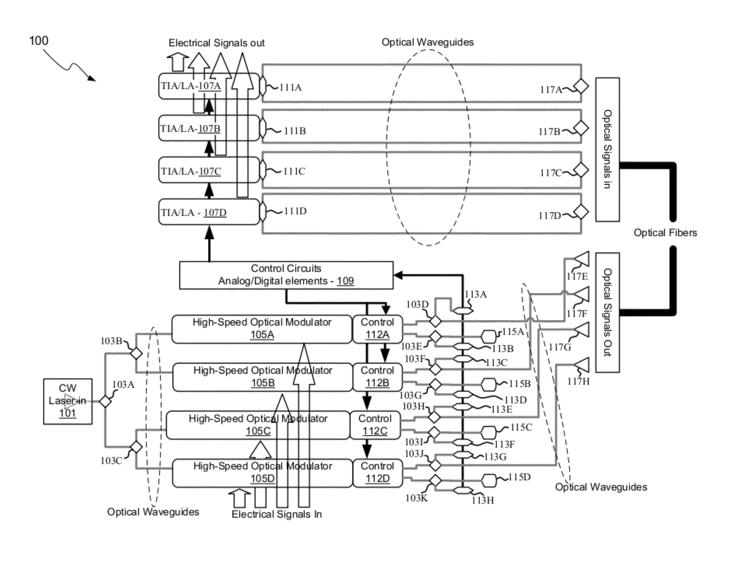
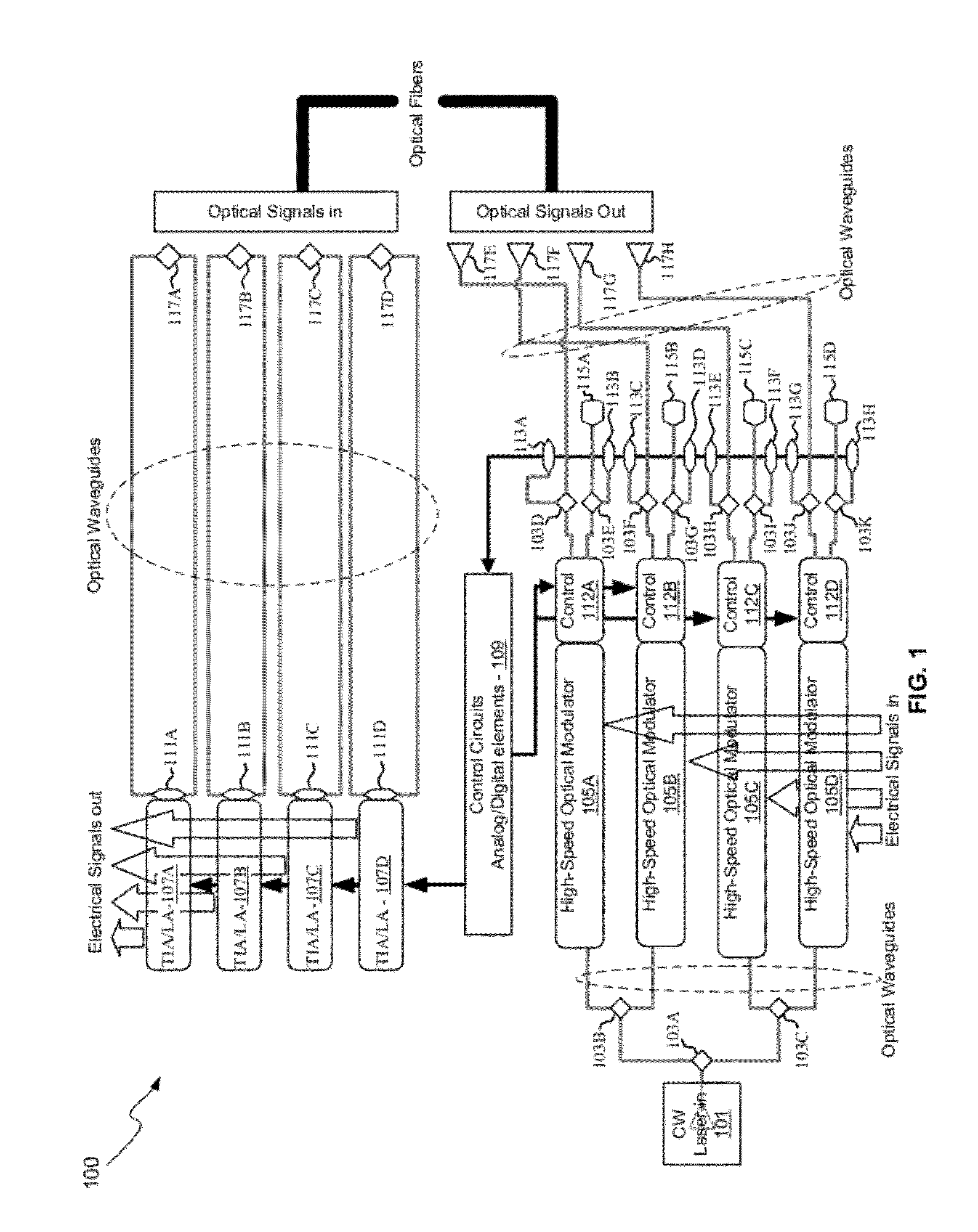
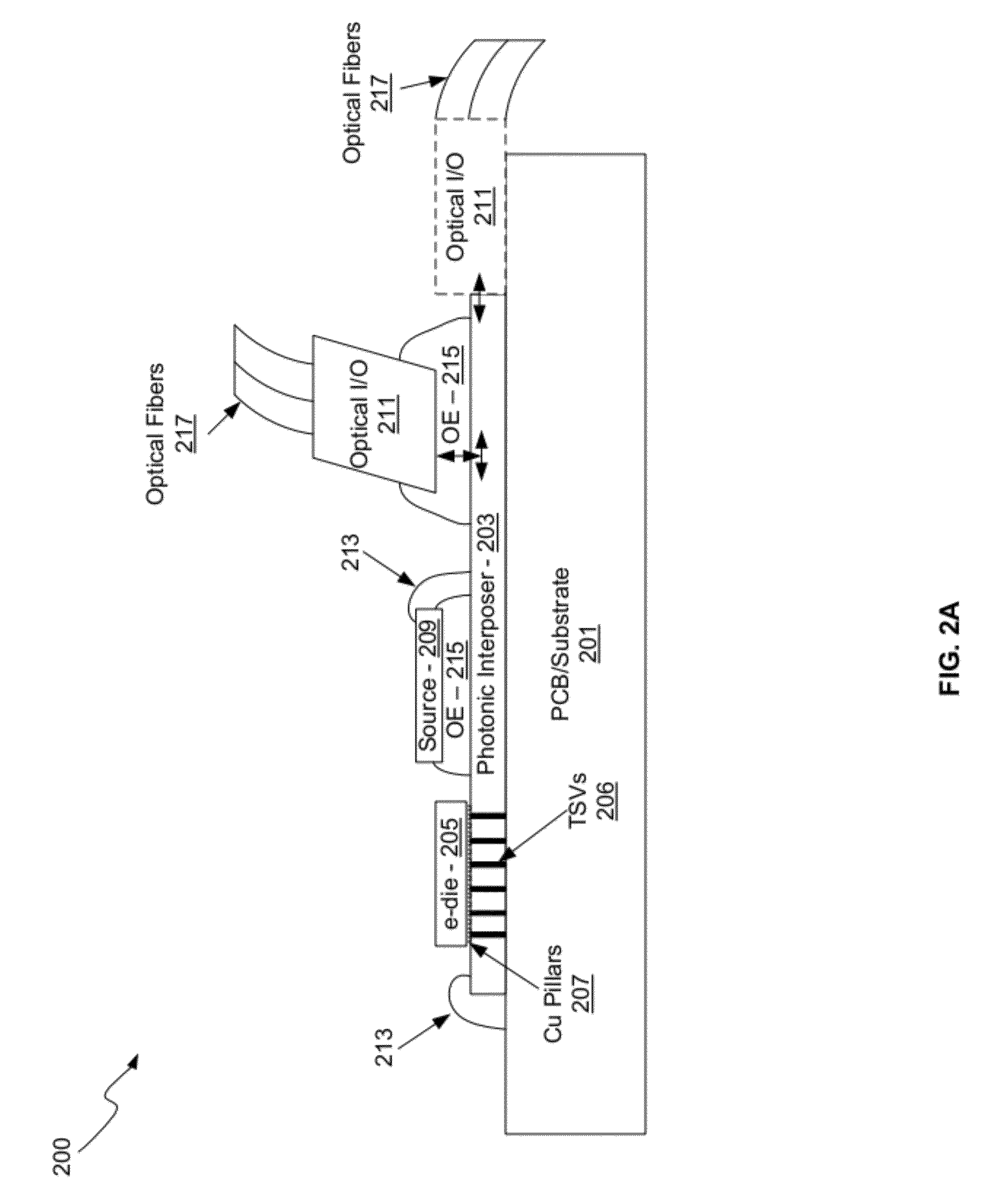
- A photonic interposer system that integrates silicon photonic devices with CMOS electronics, using Mach-Zehnder interferometer modulators, photodetectors, and grating couplers to process and transmit continuous-wave optical signals, enabling high-speed communication through optical waveguides and copper pillars, allowing independent optimization of electronic and photonic performance.

Standardization Framework for Photonic Network Components
The establishment of a comprehensive standardization framework for photonic network components represents a critical foundation for advancing photonics interposer technology and enabling accurate network latency evaluations. Current standardization efforts are fragmented across multiple organizations, including IEEE 802.3, ITU-T, and the Optical Internetworking Forum, each addressing different aspects of photonic integration without a unified approach specifically targeting interposer technologies.
The framework must encompass standardized interfaces for photonic interposers, defining precise specifications for optical coupling efficiency, insertion loss parameters, and crosstalk mitigation requirements. These standards should establish minimum performance thresholds for latency-critical applications, with specific metrics for propagation delay variations and signal integrity maintenance across different wavelength channels.
Mechanical standardization plays an equally important role, requiring standardized form factors, connector specifications, and thermal management protocols for photonic interposers. The framework should define standard footprints compatible with existing electronic packaging infrastructure while accommodating the unique requirements of optical signal routing and processing.
Testing and validation protocols constitute another essential component, establishing standardized methodologies for measuring latency performance, optical loss characteristics, and reliability parameters. These protocols must include standardized test equipment specifications and measurement procedures to ensure consistent evaluation across different manufacturers and deployment scenarios.
Interoperability standards are crucial for enabling seamless integration between photonic interposers from different vendors and existing network infrastructure. The framework should define standard communication protocols, control interfaces, and management systems that facilitate plug-and-play deployment while maintaining optimal latency performance.
The standardization framework must also address emerging requirements for artificial intelligence and machine learning applications, where ultra-low latency photonic interconnects become critical performance differentiators. This includes establishing standards for burst-mode operation, adaptive routing capabilities, and real-time performance monitoring interfaces that enable dynamic network optimization based on latency requirements.
Performance Benchmarking Methods for Photonic Latency
Performance benchmarking for photonic latency requires specialized methodologies that account for the unique characteristics of optical signal propagation and processing. Traditional electronic benchmarking approaches prove inadequate when evaluating photonic interposers due to fundamental differences in signal transmission mechanisms and timing behaviors.
The primary benchmarking framework centers on end-to-end latency measurement, encompassing optical-electrical-optical conversion delays, waveguide propagation times, and switching fabric latencies. High-precision timing equipment capable of sub-nanosecond resolution becomes essential, typically employing optical time-domain reflectometry and coherent detection systems to capture accurate temporal measurements across the photonic pathway.
Standardized test patterns play a crucial role in establishing consistent evaluation criteria. These patterns must account for wavelength-dependent variations, optical power levels, and modulation formats specific to photonic implementations. The benchmarking process requires careful consideration of environmental factors including temperature stability and mechanical vibrations that can significantly impact optical path lengths and signal integrity.
Comparative analysis methodologies involve establishing baseline measurements against conventional electronic interconnects under identical traffic conditions. This approach necessitates parallel testing environments where both photonic and electronic solutions process identical data streams, enabling direct latency comparisons while controlling for external variables.
Statistical analysis frameworks must accommodate the probabilistic nature of photonic switching and potential jitter characteristics inherent in optical systems. Monte Carlo simulations combined with real-world measurements provide comprehensive performance profiles that capture both average latency values and worst-case scenarios critical for network planning.
Scalability benchmarking represents another vital dimension, evaluating how photonic interposer performance scales with increasing port counts, wavelength channels, and traffic loads. These assessments require progressive loading tests that stress the optical switching fabric while maintaining measurement accuracy across varying operational conditions.
The benchmarking methodology must also incorporate aging effects and long-term stability assessments, as photonic components may exhibit different degradation patterns compared to electronic counterparts, potentially affecting latency characteristics over extended operational periods.
Unlock deeper insights with Patsnap Eureka Quick Research — get a full tech report to explore trends and direct your research. Try now!
Generate Your Research Report Instantly with AI Agent
Supercharge your innovation with Patsnap Eureka AI Agent Platform!