Photonics Interposers in Signal Processing: Speed Evaluation
APR 15, 20269 MIN READ
Generate Your Research Report Instantly with AI Agent
Patsnap Eureka helps you evaluate technical feasibility & market potential.
Photonic Interposer Signal Processing Background and Objectives
Photonic interposers represent a revolutionary advancement in signal processing technology, emerging from the convergence of photonics and advanced packaging solutions. These sophisticated components serve as intermediate layers that facilitate high-speed optical signal transmission between different processing units, effectively bridging the gap between electronic and photonic domains. The technology has evolved from traditional electronic interposers to address the growing demand for ultra-high bandwidth and low-latency signal processing applications.
The historical development of photonic interposers traces back to the early 2000s when researchers began exploring silicon photonics as a viable platform for integrated optical circuits. Initial efforts focused on basic optical waveguides and simple photonic components. The technology gained significant momentum around 2010 with advances in silicon-on-insulator fabrication processes and the development of efficient optical modulators and detectors.
Key evolutionary milestones include the introduction of wavelength division multiplexing capabilities, enabling multiple data channels to coexist on a single optical pathway. The integration of micro-ring resonators and photonic crystals further enhanced signal processing capabilities, allowing for more sophisticated filtering and routing functions. Recent developments have incorporated advanced materials such as indium phosphide and gallium arsenide to achieve superior performance characteristics.
The primary technical objectives driving photonic interposer development center on achieving unprecedented signal processing speeds while maintaining signal integrity across complex multi-chip architectures. Speed evaluation has become a critical focus area, as traditional electronic interconnects face fundamental physical limitations in high-frequency applications. The technology aims to overcome the bandwidth-distance product limitations inherent in copper-based interconnects.
Current research objectives emphasize the development of ultra-low latency optical switching mechanisms capable of operating at terahertz frequencies. The integration of coherent optical processing techniques represents another key objective, enabling advanced signal manipulation functions directly within the photonic domain. Additionally, the technology seeks to achieve seamless integration with existing electronic processing architectures while maintaining cost-effectiveness for commercial applications.
The overarching goal involves establishing photonic interposers as the foundation for next-generation high-performance computing systems, data centers, and telecommunications infrastructure. This includes developing standardized interfaces and protocols that enable widespread adoption across diverse application domains while ensuring scalability and reliability in demanding operational environments.
Market Demand for High-Speed Photonic Signal Processing
The global demand for high-speed photonic signal processing solutions has experienced unprecedented growth, driven by the exponential increase in data traffic and the limitations of traditional electronic systems. Data centers worldwide are struggling to meet bandwidth requirements as cloud computing, artificial intelligence, and 5G networks generate massive data volumes that exceed the capabilities of conventional copper-based interconnects. This surge in demand has created a critical market opportunity for photonic interposers that can bridge the gap between electronic processing units and optical communication systems.
Telecommunications infrastructure represents the largest market segment for high-speed photonic signal processing technologies. Network operators are actively seeking solutions that can handle terabit-scale data transmission while maintaining low latency and power consumption. The transition from 100G to 400G and beyond in optical networks has created substantial demand for photonic interposers capable of managing multiple wavelengths simultaneously and providing seamless integration between electronic and photonic domains.
The hyperscale data center market has emerged as another significant driver of demand. Major cloud service providers are investing heavily in photonic technologies to overcome the bandwidth bottlenecks in server-to-server communications and rack-to-rack connections. These facilities require photonic interposers that can support high-density optical connections while maintaining thermal stability and manufacturing scalability.
High-performance computing applications, particularly in scientific research and artificial intelligence training, are generating substantial demand for ultra-fast signal processing capabilities. These applications require photonic interposers that can handle parallel processing of optical signals with minimal signal degradation and maximum throughput efficiency.
The automotive industry's shift toward autonomous vehicles and advanced driver assistance systems has created an emerging market for photonic signal processing in LiDAR and sensor fusion applications. This sector demands photonic interposers with specific characteristics including ruggedization, cost-effectiveness, and integration with existing electronic control units.
Market growth is further accelerated by the increasing adoption of silicon photonics manufacturing processes, which have made photonic interposers more commercially viable and cost-effective for large-scale deployment across various industries.
Current State and Speed Limitations of Photonic Interposers
Photonic interposers represent a critical advancement in optical signal processing, serving as intermediate layers that facilitate high-speed data transmission between electronic and photonic components. These devices integrate optical waveguides, modulators, and photodetectors on silicon or other substrate materials, enabling seamless conversion between electrical and optical signals. Current implementations primarily utilize silicon photonics platforms, leveraging mature CMOS fabrication processes to achieve cost-effective manufacturing while maintaining compatibility with existing electronic systems.
The present state of photonic interposer technology demonstrates significant achievements in bandwidth density and power efficiency compared to traditional electronic interconnects. Leading implementations achieve data rates exceeding 100 Gbps per channel, with wavelength division multiplexing enabling aggregate throughput of several terabits per second. Silicon-on-insulator platforms dominate the landscape, offering low propagation losses of approximately 0.1-0.3 dB/cm and supporting integration densities that surpass electronic alternatives by orders of magnitude.
However, several fundamental speed limitations constrain current photonic interposer performance. Electro-optic modulation bandwidth remains restricted by RC time constants in silicon-based modulators, typically limiting single-channel speeds to 50-100 Gbps without advanced engineering techniques. Carrier mobility limitations in silicon create additional bottlenecks, particularly affecting the response time of integrated photodetectors and limiting overall system bandwidth.
Thermal management presents another critical challenge affecting speed performance. High-density photonic integration generates substantial heat loads that can shift resonant wavelengths and degrade modulation efficiency. Temperature-induced variations in refractive index create wavelength drift of approximately 0.1 nm/°C, necessitating active thermal control systems that add complexity and power consumption while potentially limiting maximum operating frequencies.
Manufacturing tolerances and process variations introduce additional speed constraints through dimensional inconsistencies that affect optical coupling efficiency and timing synchronization. Current fabrication capabilities struggle to maintain the sub-nanometer precision required for optimal high-speed performance across large-scale arrays, resulting in channel-to-channel variations that limit aggregate system performance.
Packaging and assembly challenges further compound speed limitations, as optical alignment tolerances become increasingly stringent at higher data rates. Fiber-to-chip coupling losses and reflection-induced signal degradation create practical barriers to achieving theoretical performance limits, while mechanical stability requirements for maintaining precise optical alignment add engineering complexity that can constrain maximum achievable speeds in deployed systems.
Existing Speed Optimization Solutions for Photonic Interposers
01 High-speed optical interconnect architectures in photonic interposers
Photonic interposers utilize advanced optical interconnect architectures to achieve high-speed data transmission between chips and components. These architectures incorporate waveguides, optical couplers, and routing structures that enable efficient light propagation with minimal loss. The design optimizes signal integrity and reduces latency by providing direct optical pathways between processing elements, thereby significantly increasing overall system speed compared to traditional electrical interconnects.- High-speed optical interconnect architectures in photonic interposers: Photonic interposers utilize advanced optical interconnect architectures to achieve high-speed data transmission between chips and components. These architectures incorporate waveguides, optical couplers, and routing structures that enable efficient light propagation with minimal loss. The design optimizes signal integrity and reduces latency by providing direct optical pathways between processing elements, thereby significantly increasing overall system speed compared to traditional electrical interconnects.
- Integration of silicon photonics with electronic circuits for enhanced speed: The integration of silicon photonics technology with electronic circuits on interposer platforms enables faster data transfer rates by combining the speed of light with electronic processing capabilities. This hybrid approach leverages the bandwidth advantages of optical signals while maintaining compatibility with existing semiconductor manufacturing processes. The co-integration reduces parasitic effects and interconnect delays, resulting in improved system performance and higher operational speeds.
- Advanced packaging techniques for reducing signal propagation delays: Novel packaging methodologies for photonic interposers focus on minimizing signal propagation delays through optimized physical layouts and material selection. These techniques include three-dimensional stacking, through-silicon vias, and micro-bump technologies that shorten the physical distance between optical and electrical components. The reduced path lengths and improved thermal management contribute to faster signal transmission and enhanced overall system speed.
- Wavelength division multiplexing for increased data throughput: Wavelength division multiplexing techniques implemented in photonic interposers enable multiple data channels to be transmitted simultaneously over the same optical pathway using different wavelengths of light. This approach dramatically increases the aggregate data throughput without requiring additional physical interconnects. The parallel transmission capability allows for scalable bandwidth expansion, making it possible to achieve significantly higher speeds in data-intensive applications.
- Low-latency optical switching and routing mechanisms: Photonic interposers incorporate low-latency optical switching and routing mechanisms that enable rapid reconfiguration of data paths and dynamic bandwidth allocation. These mechanisms utilize electro-optic modulators, optical switches, and intelligent routing algorithms to minimize switching times and optimize data flow. The fast switching capabilities reduce bottlenecks and enable real-time adaptation to varying traffic patterns, thereby maintaining high-speed performance across diverse operating conditions.
02 Integration of silicon photonics with electronic circuits for enhanced speed
The integration of silicon photonics technology with electronic circuits on interposer platforms enables faster data transfer rates by combining the speed of light with electronic processing capabilities. This hybrid approach leverages the bandwidth advantages of optical signals while maintaining compatibility with existing semiconductor manufacturing processes. The co-integration reduces parasitic effects and interconnect delays, resulting in improved system performance and higher operational speeds.Expand Specific Solutions03 Advanced packaging techniques for reducing signal propagation delays
Novel packaging methodologies for photonic interposers focus on minimizing signal propagation delays through optimized physical layouts and material selection. These techniques include three-dimensional stacking, through-silicon vias, and micro-bump technologies that shorten the physical distance between optical and electrical components. The reduced path lengths and improved thermal management contribute to faster signal transmission and enhanced overall system speed.Expand Specific Solutions04 Wavelength division multiplexing for increased data throughput
Wavelength division multiplexing techniques implemented in photonic interposers enable multiple data channels to be transmitted simultaneously over the same optical pathway using different wavelengths of light. This approach dramatically increases the aggregate data throughput without requiring additional physical interconnects. The parallel transmission capability allows for scalable bandwidth expansion, making it possible to achieve significantly higher speeds in data-intensive applications.Expand Specific Solutions05 Low-latency optical switching and routing mechanisms
Photonic interposers incorporate low-latency optical switching and routing mechanisms that enable rapid reconfiguration of data paths and dynamic bandwidth allocation. These mechanisms utilize electro-optic modulators, optical switches, and intelligent routing algorithms to minimize switching times and optimize data flow. The fast switching capabilities reduce bottlenecks and enable real-time adaptation to varying traffic patterns, thereby maintaining high-speed performance across diverse operating conditions.Expand Specific Solutions
Key Players in Photonic Interposer and Signal Processing Industry
The photonics interposers market for signal processing is in an emerging growth phase, driven by increasing demand for high-speed data transmission and AI computing requirements. The market demonstrates significant potential with established technology giants like Sony, Huawei, TSMC, and Fujitsu investing heavily alongside specialized players such as Lightmatter and Shanghai Xizhi Technology. Technology maturity varies considerably across the competitive landscape - while companies like Canon, Toshiba, and STMicroelectronics leverage their semiconductor expertise, pure-play photonics firms like Lightmatter are pushing cutting-edge innovations in light-based computing. Traditional telecommunications leaders including Ericsson, ZTE, and Fiberhome are integrating photonic solutions into their infrastructure offerings. The presence of research institutions like MIT and UESTC indicates strong academic-industry collaboration, suggesting the technology is transitioning from research to commercial viability with accelerating development cycles.
Lightmatter, Inc.
Technical Solution: Lightmatter has developed revolutionary photonic interposer technology that enables ultra-high-speed signal processing by integrating optical and electronic components on a single substrate. Their photonic interconnect solutions achieve data transmission speeds exceeding 1 Tbps while reducing power consumption by up to 90% compared to traditional electronic interconnects. The company's photonic interposer architecture utilizes silicon photonics technology to create dense optical routing networks that can handle massive parallel data processing tasks. Their innovative approach combines wavelength division multiplexing with advanced modulation techniques to maximize bandwidth efficiency in AI and datacenter applications.
Strengths: Industry-leading power efficiency and bandwidth capabilities, proven commercial deployment. Weaknesses: High manufacturing complexity and cost, limited ecosystem compatibility.
Huawei Technologies Co., Ltd.
Technical Solution: Huawei has invested heavily in photonic interposer technology for next-generation telecommunications and data processing systems. Their approach focuses on integrating silicon photonic components with advanced CMOS electronics to create high-performance signal processing platforms. The company's photonic interposer solutions target 5G/6G infrastructure and cloud computing applications, offering multi-terabit processing capabilities with significantly reduced latency compared to traditional electronic systems. Their technology incorporates advanced optical switching matrices and high-speed photodetectors to enable real-time signal processing for telecommunications networks.
Strengths: Strong R&D capabilities and telecommunications market presence, comprehensive system integration expertise. Weaknesses: Geopolitical restrictions limiting global market access, dependency on external foundry capabilities.
Core Speed Enhancement Patents in Photonic Signal Processing
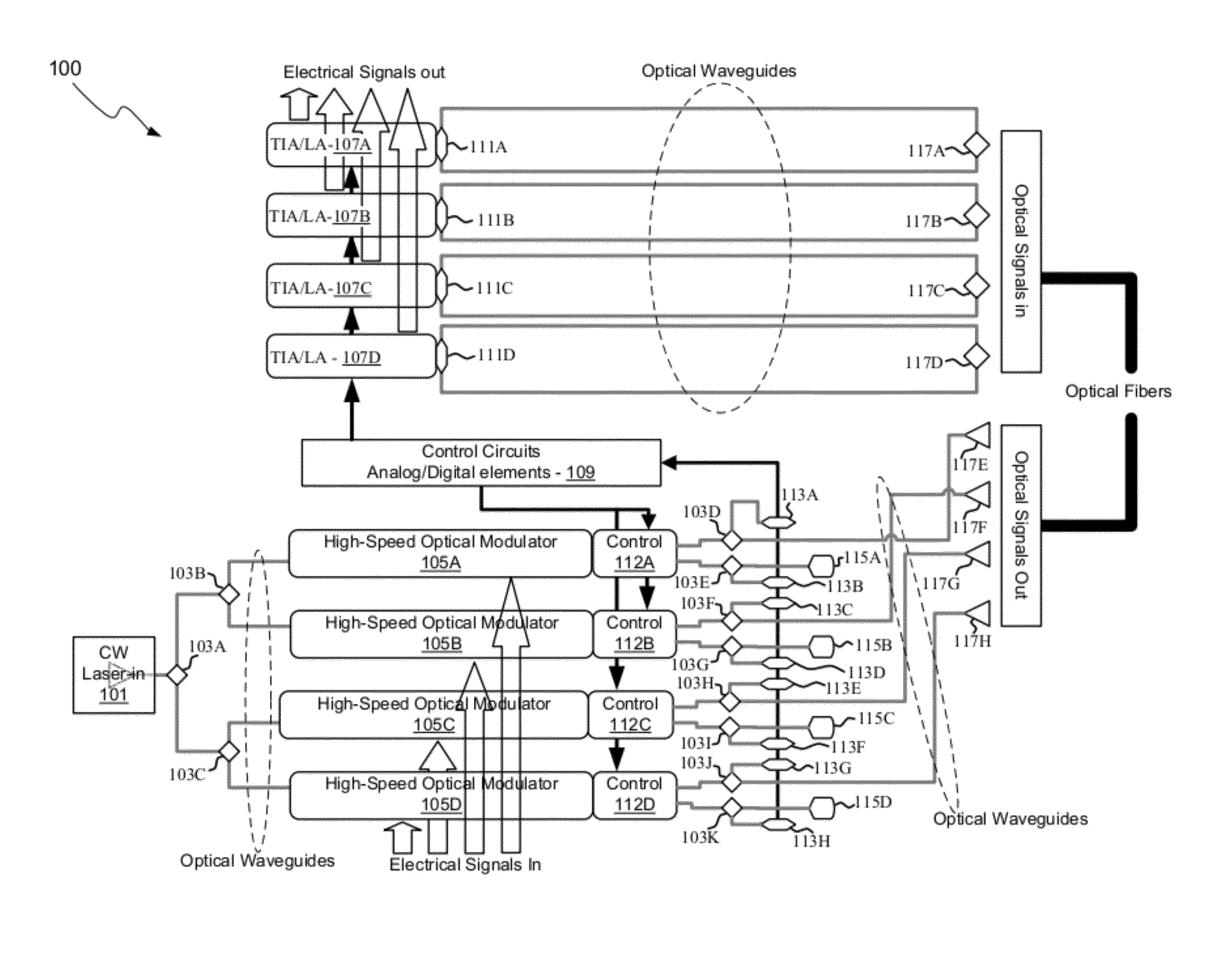
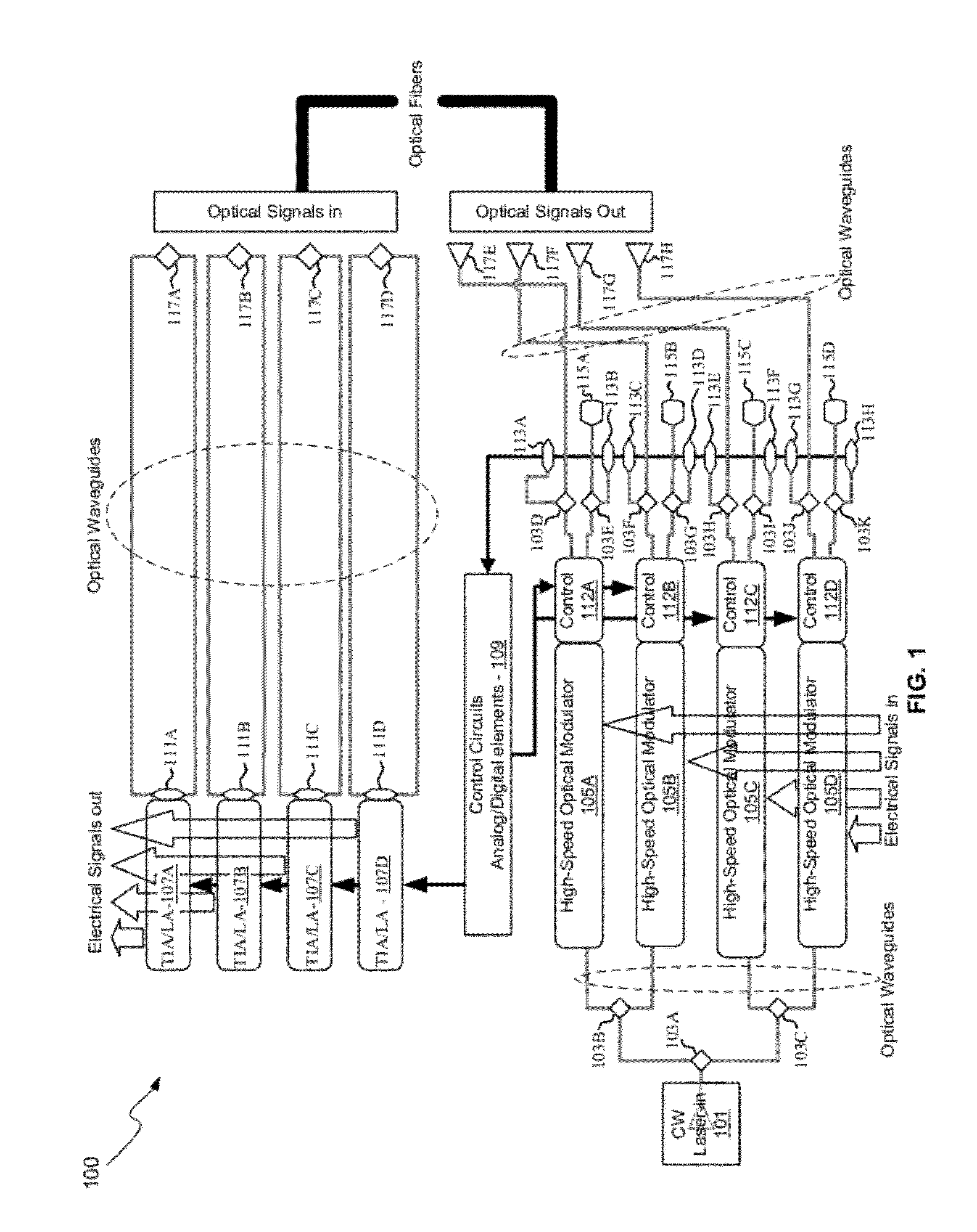
Method And System For A Photonic Interposer
PatentActiveUS20120177381A1
Innovation
- A photonic interposer system that integrates silicon photonic devices with CMOS electronics, using Mach-Zehnder interferometer modulators, photodetectors, and grating couplers to process and transmit continuous-wave optical signals, enabling high-speed communication through optical waveguides and copper pillars, allowing independent optimization of electronic and photonic performance.
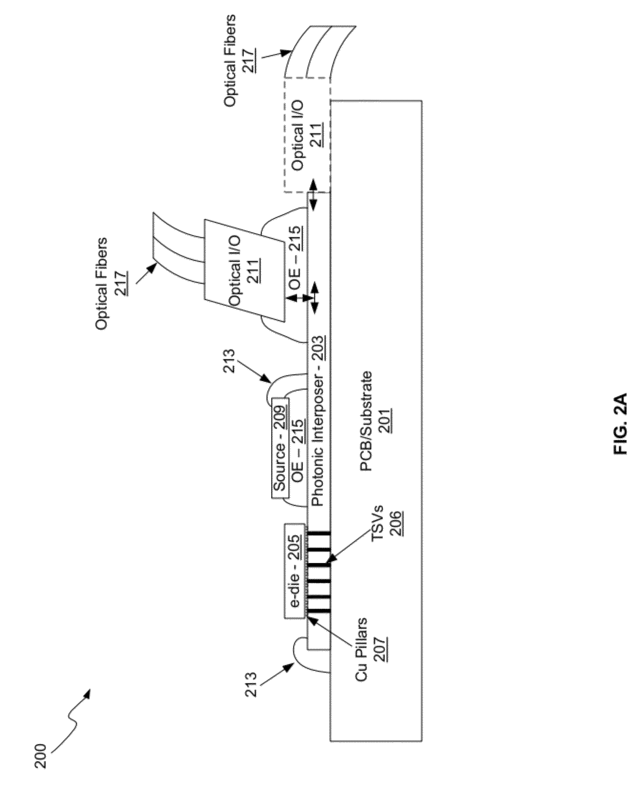

Method And System For A Photonic Interposer
PatentActiveUS20190363797A1
Innovation
- A photonic interposer system that integrates silicon photonic devices with CMOS electronics, using Mach-Zehnder interferometer modulators and grating couplers to process and transmit continuous-wave optical signals, enabling high-speed communication by converting electrical signals to optical and vice versa through copper pillars and optical fibers.


Performance Benchmarking Standards for Photonic Devices
The establishment of comprehensive performance benchmarking standards for photonic devices represents a critical foundation for evaluating photonics interposers in signal processing applications. Current industry practices lack unified metrics and standardized testing protocols, creating significant challenges in comparing device performance across different manufacturers and technological approaches. The absence of consistent benchmarking frameworks has hindered the widespread adoption of photonic solutions in high-speed signal processing systems.
Standardization efforts must address multiple performance dimensions including optical insertion loss, electrical-to-optical conversion efficiency, bandwidth characteristics, and thermal stability. Key parameters requiring standardized measurement protocols include signal-to-noise ratio degradation, crosstalk between adjacent channels, and power consumption metrics under various operating conditions. These standards should encompass both static performance characteristics and dynamic behavior under real-world signal processing scenarios.
International organizations such as IEEE and IEC have initiated preliminary frameworks for photonic device characterization, yet specific standards for interposer applications remain underdeveloped. The complexity arises from the hybrid nature of photonic interposers, which integrate optical and electrical components requiring dual-domain performance evaluation methodologies. Current proposals suggest adopting eye diagram analysis, bit error rate measurements, and jitter characterization as fundamental benchmarking tools.
Temperature cycling protocols and accelerated aging tests constitute essential components of comprehensive benchmarking standards. These reliability assessments must account for the unique thermal characteristics of photonic materials and their interaction with electronic substrates. Standardized environmental testing conditions should include humidity exposure, mechanical stress evaluation, and electromagnetic interference susceptibility measurements.
The development of automated testing equipment and calibrated measurement systems represents another crucial aspect of benchmarking standardization. Reference devices and certified measurement procedures ensure reproducibility across different testing facilities and enable meaningful performance comparisons. Industry consensus on measurement uncertainties and statistical analysis methods will facilitate accurate performance validation and quality assurance processes for next-generation photonic interposer technologies.
Thermal Management Challenges in High-Speed Photonic Systems
Thermal management represents one of the most critical engineering challenges in high-speed photonic systems, particularly when implementing photonic interposers for signal processing applications. As data transmission rates exceed 100 Gbps per channel and system integration densities continue to increase, the heat generation from both optical and electronic components creates significant performance bottlenecks that directly impact signal processing speed and reliability.
The primary thermal challenge stems from the inherent heat generation in high-speed modulators, photodetectors, and driver electronics integrated within photonic interposers. Silicon photonic modulators operating at speeds beyond 50 Gbps typically generate substantial heat due to carrier injection and depletion processes, while germanium photodetectors exhibit temperature-dependent responsivity that can degrade signal quality. Additionally, the co-packaged electronic components, including transimpedance amplifiers and digital signal processors, contribute significant thermal loads that can exceed 10 watts per square centimeter in dense integration scenarios.
Temperature variations create cascading effects on system performance, with wavelength drift in laser sources and ring resonators being particularly problematic. A temperature increase of just 1°C can cause wavelength shifts of approximately 0.1 nm in silicon photonic devices, leading to crosstalk and signal degradation in wavelength division multiplexing systems. This thermal sensitivity necessitates precise temperature control within ±0.1°C for optimal performance, presenting substantial engineering challenges in compact form factors.
Current thermal management approaches include advanced heat sink designs, micro-channel cooling systems, and thermal interface materials optimized for photonic applications. However, these solutions often introduce trade-offs between cooling efficiency and system complexity, with some active cooling methods consuming up to 20% of total system power. The integration of thermal monitoring and feedback control systems adds additional complexity while being essential for maintaining performance stability across varying operational conditions.
Emerging thermal management strategies focus on novel materials such as diamond heat spreaders, advanced thermal interface materials with enhanced conductivity, and innovative packaging architectures that optimize heat dissipation paths. These approaches aim to address the fundamental thermal limitations that currently constrain the scalability of high-speed photonic signal processing systems.
Unlock deeper insights with Patsnap Eureka Quick Research — get a full tech report to explore trends and direct your research. Try now!
Generate Your Research Report Instantly with AI Agent
Supercharge your innovation with Patsnap Eureka AI Agent Platform!