

Photonics Interposers vs Silicon: Efficiency Comparison
APR 15, 20269 MIN READ
Generate Your Research Report Instantly with AI Agent
PatSnap Eureka helps you evaluate technical feasibility & market potential.
Photonics Interposer Technology Background and Objectives
Photonics interposer technology represents a paradigm shift in high-performance computing and data communication systems, emerging as a critical solution to address the fundamental limitations of traditional silicon-based interconnects. This technology leverages optical signals for data transmission between electronic components, offering unprecedented bandwidth capabilities and energy efficiency compared to conventional electrical interconnections.
The evolution of photonics interposers stems from the growing demand for faster data processing and transmission in modern computing architectures. As semiconductor scaling approaches physical limits and Moore's Law faces increasing challenges, the industry has recognized the need for alternative approaches to maintain performance growth trajectories. Photonics interposers bridge this gap by integrating optical waveguides, modulators, and photodetectors directly into chip-level packaging solutions.
Historical development of this technology traces back to early optical communication research in the 1960s, with significant acceleration occurring in the past two decades. Key milestones include the demonstration of silicon photonics integration in the early 2000s, followed by successful implementation of on-chip optical interconnects and the development of hybrid electronic-photonic systems. Recent advances have focused on reducing manufacturing costs and improving integration density.
The primary technical objectives driving photonics interposer development center on achieving superior bandwidth density, reduced power consumption, and enhanced signal integrity compared to silicon-based solutions. Current research targets include developing low-loss optical coupling mechanisms, creating efficient electro-optic conversion interfaces, and establishing reliable manufacturing processes for large-scale production.
Performance objectives encompass achieving data transmission rates exceeding 100 Gbps per channel while maintaining power efficiency below 1 pJ/bit. Additionally, the technology aims to support massive parallel processing architectures required for artificial intelligence, machine learning, and high-performance computing applications where traditional silicon interconnects create significant bottlenecks.
Manufacturing and integration goals focus on developing cost-effective production methods that can compete with established silicon technologies while providing superior performance characteristics. This includes advancing wafer-level integration techniques, improving yield rates, and establishing standardized packaging solutions that facilitate widespread industry adoption across diverse application domains.
Market Demand for High-Performance Interconnect Solutions
The global demand for high-performance interconnect solutions has reached unprecedented levels, driven by the exponential growth of data-intensive applications across multiple sectors. Cloud computing infrastructure, artificial intelligence workloads, and high-performance computing systems require interconnect technologies that can handle massive data throughput while maintaining energy efficiency. Traditional copper-based interconnects are increasingly unable to meet these demanding requirements, particularly in terms of bandwidth density and power consumption.
Data centers represent the largest market segment driving interconnect innovation, as operators seek solutions to address the bandwidth bottleneck between processors, memory, and storage systems. The proliferation of machine learning applications and real-time analytics has created an urgent need for interconnect solutions that can support terabit-scale data rates with minimal latency. This demand is further amplified by the growing adoption of disaggregated computing architectures, where processing, memory, and storage resources are distributed across multiple nodes.
Telecommunications infrastructure modernization presents another significant market driver, particularly with the deployment of advanced wireless networks and edge computing facilities. Network equipment manufacturers require interconnect solutions that can handle the increased data volumes while reducing overall system power consumption and footprint. The transition toward software-defined networking and network function virtualization has intensified the need for flexible, high-bandwidth interconnect architectures.
The automotive and aerospace industries are emerging as important market segments, driven by the development of autonomous systems and advanced driver assistance technologies. These applications demand interconnect solutions that can process sensor data in real-time while meeting stringent reliability and environmental requirements. The growing complexity of electronic systems in these sectors has created opportunities for advanced interconnect technologies that can provide both high performance and robust operation.
Market analysis indicates that traditional silicon-based interconnect solutions face fundamental physical limitations in meeting future bandwidth and efficiency requirements. The industry is actively seeking alternative approaches that can overcome these constraints while providing cost-effective scalability. This market pressure has intensified research and development efforts in photonic interconnect technologies, which offer the potential to address both bandwidth and energy efficiency challenges simultaneously.
The competitive landscape reflects this market demand, with significant investments flowing into companies developing next-generation interconnect solutions. Market participants are focusing on technologies that can provide substantial improvements in bandwidth density, energy efficiency, and integration capabilities compared to existing silicon-based approaches.
Current State of Photonics vs Silicon Interposer Technologies
Silicon interposer technology has reached significant maturity in the semiconductor industry, establishing itself as the dominant solution for advanced packaging applications. Current silicon interposers leverage well-established CMOS fabrication processes, enabling feature sizes down to 2-5 micrometers for through-silicon vias (TSVs) and redistribution layers. Major foundries including TSMC, Samsung, and Intel have developed robust manufacturing capabilities, with production volumes reaching hundreds of thousands of units annually for high-performance computing and mobile applications.
The electrical performance of silicon interposers demonstrates excellent signal integrity for frequencies up to 56 Gbps, with power delivery networks capable of supporting multi-core processors and high-bandwidth memory interfaces. Thermal management remains a critical consideration, as silicon's moderate thermal conductivity of 150 W/mK requires careful design optimization for heat dissipation in dense packaging configurations.
Photonics interposer technology represents an emerging paradigm that integrates optical waveguides, modulators, and photodetectors within the interposer substrate. Current implementations primarily utilize silicon photonics platforms, combining silicon-on-insulator (SOI) wafers with specialized fabrication processes to create optical interconnects alongside electrical pathways. Leading research institutions and companies including Intel, IBM, and Luxtera have demonstrated functional prototypes achieving data rates exceeding 100 Gbps per optical channel.
The manufacturing ecosystem for photonics interposers remains in early development stages, with limited commercial foundry availability compared to traditional silicon interposers. Current production capabilities are primarily concentrated in specialized facilities with hybrid integration processes that combine electronic and photonic components through advanced packaging techniques such as flip-chip bonding and wafer-level integration.
Performance characteristics of photonics interposers show promising advantages in bandwidth density and power efficiency for long-distance on-package communications. Optical links demonstrate significantly lower power consumption per bit transmitted compared to electrical interconnects, particularly for distances exceeding several millimeters. However, the technology faces challenges in achieving cost-effective integration of optical components, including laser sources, which often require external coupling or hybrid integration approaches.
Manufacturing yield and reliability metrics for photonics interposers currently lag behind silicon interposer benchmarks, primarily due to the complexity of optical component integration and the sensitivity of photonic devices to process variations. Temperature stability and packaging-induced stress effects on optical performance represent ongoing technical challenges requiring specialized design methodologies and materials engineering solutions.
Existing Photonics and Silicon Interposer Solutions
01 Optical coupling and alignment structures in photonic interposers
Photonic interposers can incorporate specialized optical coupling structures and alignment features to improve light transmission efficiency between optical components. These structures include waveguide couplers, grating couplers, and precision alignment marks that enable accurate positioning of optical elements. Advanced coupling mechanisms reduce insertion loss and improve signal integrity by minimizing optical path misalignment. The integration of passive alignment features during fabrication ensures consistent performance across multiple devices.- Optical coupling and alignment structures in photonic interposers: Photonic interposers can incorporate specialized optical coupling structures and precise alignment features to improve light transmission efficiency between optical components. These structures include waveguide couplers, grating couplers, and micro-lens arrays that facilitate efficient optical signal transfer. Advanced alignment mechanisms such as passive alignment features and self-alignment structures help minimize coupling losses and improve overall system performance.
- Integration of electronic and photonic components on interposer substrates: Photonic interposers enable the co-integration of electronic and photonic components on a single substrate platform, reducing signal path lengths and improving energy efficiency. This hybrid integration approach allows for optimized placement of optical and electrical elements, minimizing conversion losses and parasitic effects. The interposer architecture facilitates high-density integration while maintaining thermal management and signal integrity.
- Waveguide design and material optimization for reduced optical losses: The efficiency of photonic interposers can be enhanced through optimized waveguide geometries and material selection that minimize propagation losses and scattering. Low-loss dielectric materials and optimized core-cladding configurations improve light confinement and transmission. Advanced fabrication techniques enable the creation of smooth waveguide surfaces and controlled refractive index profiles that reduce attenuation and improve signal quality.
- Thermal management and packaging solutions for photonic interposers: Effective thermal management strategies are critical for maintaining photonic interposer efficiency under operating conditions. Integrated heat dissipation structures, thermal interface materials, and packaging designs help maintain optimal operating temperatures for photonic components. These solutions prevent thermal-induced wavelength drift and maintain stable optical performance while supporting high-power operation.
- Multi-layer interconnect architectures for enhanced signal routing: Advanced multi-layer photonic interposer designs enable complex optical routing with improved efficiency through vertical and horizontal integration of optical pathways. These architectures utilize through-silicon vias, multi-level waveguide layers, and three-dimensional optical interconnects to optimize signal distribution. The layered approach reduces crosstalk, minimizes insertion losses, and enables compact device footprints while maintaining high bandwidth density.
02 Material selection and waveguide design for loss reduction
The efficiency of photonic interposers is significantly influenced by the choice of materials and waveguide geometries. Low-loss dielectric materials and optimized waveguide cross-sections minimize propagation losses and improve overall transmission efficiency. Silicon-based and polymer-based waveguide structures can be engineered with specific refractive index profiles to enhance mode confinement and reduce scattering losses. Advanced material processing techniques enable the fabrication of high-quality optical interfaces with minimal surface roughness.Expand Specific Solutions03 Thermal management and packaging for photonic interposers
Effective thermal management is critical for maintaining the efficiency of photonic interposers, as temperature variations can affect optical performance and signal quality. Integrated heat dissipation structures, thermal interface materials, and packaging designs help maintain stable operating temperatures. Advanced packaging techniques incorporate thermal vias, heat spreaders, and active cooling mechanisms to manage heat generated by co-packaged electronic and photonic components. Proper thermal design prevents wavelength drift and maintains consistent optical coupling efficiency.Expand Specific Solutions04 Integration of active optical components and electrical interfaces
Photonic interposers can integrate active optical components such as modulators, detectors, and light sources to create complete optical systems with enhanced functionality. The co-integration of electrical and optical interfaces on a single substrate reduces interconnect losses and improves overall system efficiency. Advanced fabrication processes enable the monolithic or hybrid integration of III-V semiconductor devices with silicon photonic circuits. Efficient electrical-to-optical and optical-to-electrical conversion mechanisms are essential for maximizing data transmission rates and minimizing power consumption.Expand Specific Solutions05 Multi-layer and 3D photonic interposer architectures
Three-dimensional and multi-layer photonic interposer designs enable higher integration density and improved routing flexibility for complex optical systems. Vertical optical interconnects and through-substrate vias allow signals to be routed between different layers, reducing footprint and improving efficiency. Advanced fabrication techniques such as wafer bonding and layer transfer enable the creation of multi-tier photonic structures with minimal optical loss. These architectures support higher bandwidth density and enable more efficient use of substrate area for large-scale photonic integration.Expand Specific Solutions
Key Players in Photonics and Silicon Interposer Markets
The photonics interposers versus silicon efficiency comparison represents an emerging technology sector in the early growth stage, driven by increasing demand for high-performance computing and data center applications. The market is experiencing rapid expansion as traditional silicon interconnects face bandwidth and power consumption limitations. Technology maturity varies significantly across players, with established semiconductor giants like Taiwan Semiconductor Manufacturing, Samsung Electronics, and IBM leading in silicon photonics integration, while specialized companies such as Lightmatter and Lumentum Operations focus on pure photonic solutions. Chinese entities including Huawei Technologies, Shanghai Institute of Microsystem & Information Technology, and Shanghai Jiao Tong University are heavily investing in photonic interposer development to achieve technological independence. The competitive landscape shows a hybrid approach emerging, where companies like Hewlett Packard Enterprise and Oracle International are exploring both silicon and photonic solutions to optimize efficiency based on specific application requirements.
Huawei Technologies Co., Ltd.
Technical Solution: Huawei has invested heavily in both silicon and photonic interposer technologies for telecommunications and computing applications. Their silicon interposer solutions focus on high-density packaging for 5G infrastructure and data center equipment, providing reliable electrical interconnects with proven manufacturing scalability. Additionally, Huawei is developing photonic interposer technology for next-generation optical communication systems, targeting applications where bandwidth and power efficiency are critical. Their research indicates that photonic interposers can deliver up to 3x better power efficiency compared to traditional silicon solutions in optical networking equipment, while maintaining the cost advantages of silicon for high-volume production.
Strengths: Strong telecommunications expertise, comprehensive R&D capabilities, integration with networking equipment, cost optimization focus. Weaknesses: Geopolitical constraints affecting global market access, technology transfer limitations.
Taiwan Semiconductor Manufacturing Co., Ltd.
Technical Solution: TSMC has developed advanced silicon interposer technology as part of their Chip-on-Wafer-on-Substrate (CoWoS) packaging platform. Their silicon interposers provide high-density interconnects for heterogeneous integration, enabling multiple chips to communicate through fine-pitch redistribution layers. TSMC's silicon-based approach offers proven reliability and cost-effectiveness for high-volume manufacturing, with interposers supporting thousands of connections per square millimeter. The technology enables 3D stacking and heterogeneous integration while maintaining compatibility with standard semiconductor processes, making it suitable for applications ranging from high-performance computing to mobile processors.
Strengths: Mature manufacturing processes, proven reliability, cost-effective for high volumes, extensive ecosystem support. Weaknesses: Limited bandwidth compared to photonic solutions, higher power consumption for data-intensive applications.
Core Innovations in Photonic Interposer Efficiency
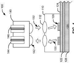
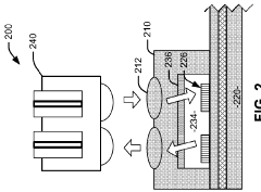
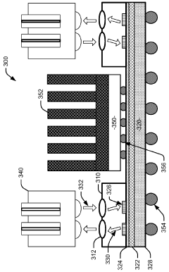
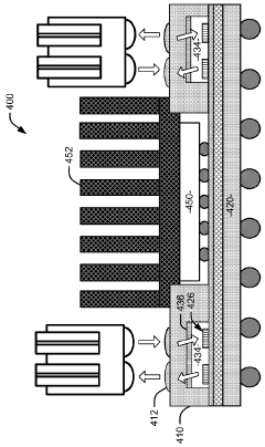
Photonic interposer with wafer bonded microlenses
PatentWO2016068876A1
Innovation
- The integration of wafer-bonded microlenses with grating couplers and expanded beam fiber optic connectors, leveraging MEMS fabrication techniques for precise alignment and signal collimation, reduces the need for active alignment of multiple optical elements, facilitating high-precision signal transfer and improved assembly efficiency.
Galvanic optocoupler and method of making
PatentInactiveUS20080173879A1
Innovation
- A galvanic optocoupler is designed with a phototransistor as the photodetector and a passivation layer serving as the galvanic insulation, using a silicon substrate and integrating an LED with a silicon oxide layer enriched with silicon, eliminating the need for expensive materials like Indium Tin Oxide and simplifying the integration process.


Manufacturing Standards for Photonic Interposers
The manufacturing of photonic interposers requires adherence to stringent standards that significantly differ from traditional silicon semiconductor fabrication processes. Current industry standards are primarily governed by IEEE 802.3 specifications for optical interconnects and IEC 62496 series for optoelectronic devices, though dedicated photonic interposer standards are still evolving. The Optical Internetworking Forum (OIF) and the IEEE P802.3 working groups are actively developing comprehensive manufacturing guidelines specifically addressing the unique requirements of photonic integration platforms.
Dimensional tolerances represent one of the most critical manufacturing parameters, with alignment accuracy requirements typically demanding sub-micron precision for optical coupling efficiency. Standard fabrication processes must maintain waveguide core positioning within ±0.1 μm tolerances, while surface roughness specifications require Ra values below 1 nm to minimize optical scattering losses. These tolerances are substantially tighter than conventional silicon interposer requirements, necessitating specialized metrology equipment and process control methodologies.
Material quality standards encompass both optical and mechanical properties, with refractive index uniformity specifications typically requiring variations less than ±0.001 across the substrate. Silicon-on-insulator (SOI) wafers used for photonic applications must meet enhanced crystalline quality standards, with defect densities below 0.1 cm⁻² for the device layer. The buried oxide layer thickness uniformity must be maintained within ±2% to ensure consistent optical confinement characteristics across the interposer.
Process standardization covers critical manufacturing steps including lithography, etching, and packaging procedures. Advanced lithography techniques such as electron beam lithography or deep UV photolithography are standardized for feature sizes below 100 nm, essential for efficient photonic device fabrication. Dry etching processes require precise control of sidewall angles, typically maintained within ±2° to optimize optical mode confinement and minimize coupling losses.
Quality assurance protocols incorporate both electrical and optical testing methodologies, with insertion loss measurements, crosstalk characterization, and bandwidth verification forming the core testing suite. Reliability standards mandate accelerated aging tests under elevated temperature and humidity conditions, ensuring long-term performance stability comparable to traditional electronic components while meeting the additional requirements of optical signal integrity.
Cost-Performance Trade-offs in Interposer Selection
The selection of interposers in high-performance computing and data center applications involves critical cost-performance trade-offs that significantly impact system economics and operational efficiency. Photonic interposers, while offering superior bandwidth density and energy efficiency per bit transmitted, typically command premium pricing due to specialized manufacturing processes and lower production volumes. The initial capital expenditure for photonic solutions can be 2-3 times higher than silicon alternatives, creating substantial upfront investment barriers for many organizations.
Silicon interposers maintain cost advantages through mature semiconductor manufacturing infrastructure and economies of scale. The established fabrication ecosystem enables predictable pricing models and shorter lead times, making silicon solutions attractive for cost-sensitive applications. However, the total cost of ownership calculation reveals more nuanced considerations when factoring in power consumption, cooling requirements, and system scalability over operational lifespans.
Performance metrics demonstrate distinct trade-off patterns across different application scenarios. Photonic interposers excel in bandwidth-intensive applications where data throughput requirements exceed 100 Gbps per channel, delivering superior signal integrity and reduced latency. The energy efficiency advantages become particularly pronounced in large-scale deployments where power consumption directly impacts operational expenses and thermal management costs.
Silicon interposers offer competitive performance for moderate bandwidth requirements while providing greater design flexibility and integration options with existing electronic systems. The performance-per-dollar ratio favors silicon solutions in applications where maximum bandwidth utilization is not critical, such as traditional computing workloads and cost-optimized data center configurations.
Market dynamics further influence cost-performance considerations through technology maturity curves and supply chain stability. Silicon interposer pricing benefits from established supplier networks and competitive manufacturing capacity, while photonic solutions face potential supply constraints and price volatility during market expansion phases. Long-term cost projections suggest convergence trends as photonic manufacturing scales and silicon approaches physical performance limits, fundamentally reshaping the cost-performance landscape for future interposer selection decisions.
Unlock deeper insights with PatSnap Eureka Quick Research — get a full tech report to explore trends and direct your research. Try now!
Generate Your Research Report Instantly with AI Agent
Supercharge your innovation with PatSnap Eureka AI Agent Platform!