

Understanding Electron Beam Control for Better Process Outcomes
MAR 18, 20269 MIN READ
Generate Your Research Report Instantly with AI Agent
PatSnap Eureka helps you evaluate technical feasibility & market potential.
Electron Beam Technology Background and Objectives
Electron beam technology represents a sophisticated materials processing method that harnesses the kinetic energy of accelerated electrons to achieve precise heating, melting, welding, and surface modification applications. This technology emerged in the mid-20th century as an evolution of vacuum tube technology, initially finding applications in electron microscopy before expanding into industrial manufacturing processes. The fundamental principle involves generating a focused beam of high-energy electrons in a vacuum environment, enabling unprecedented control over energy density and spatial precision.
The historical development of electron beam processing can be traced back to the 1950s when researchers first recognized the potential for using electron beams in materials processing applications. Early implementations focused on welding applications in aerospace manufacturing, where the technology's ability to create deep, narrow welds with minimal heat-affected zones proved invaluable. Over subsequent decades, the technology evolved to encompass additive manufacturing, surface treatment, and precision machining applications.
Current technological evolution trends indicate a shift toward enhanced beam control systems, real-time process monitoring, and integration with advanced automation platforms. Modern electron beam systems incorporate sophisticated deflection systems, multi-beam configurations, and adaptive control algorithms that respond to process feedback in real-time. These advancements enable manufacturers to achieve previously unattainable levels of precision and repeatability in complex manufacturing operations.
The primary technical objectives driving contemporary electron beam research focus on improving process stability, expanding material compatibility, and enhancing throughput capabilities. Key development goals include achieving sub-micron positioning accuracy, implementing predictive process control systems, and developing hybrid processing techniques that combine electron beam technology with other advanced manufacturing methods.
Future technological targets encompass the development of intelligent beam control systems capable of autonomous process optimization, integration with Industry 4.0 manufacturing frameworks, and expansion into emerging application areas such as quantum device fabrication and advanced semiconductor processing. These objectives align with broader industry trends toward digitalization, sustainability, and precision manufacturing, positioning electron beam technology as a critical enabler for next-generation manufacturing capabilities.
Market Demand for Advanced Electron Beam Processing
The global electron beam processing market is experiencing unprecedented growth driven by increasing demand for precision manufacturing across multiple industrial sectors. Semiconductor fabrication represents the largest market segment, where electron beam lithography enables the production of next-generation microprocessors and memory devices with feature sizes below 10 nanometers. The continuous miniaturization of electronic components necessitates more sophisticated electron beam control systems capable of achieving sub-nanometer positioning accuracy.
Additive manufacturing has emerged as a rapidly expanding application area for electron beam processing. Industries ranging from aerospace to medical devices are adopting electron beam melting and welding technologies for their ability to process high-performance materials including titanium alloys, superalloys, and refractory metals. The automotive sector particularly values electron beam welding for battery pack assembly in electric vehicles, where precise heat control prevents thermal damage to sensitive components.
Surface modification and coating applications represent another significant market driver. Electron beam processing enables precise control over material properties through selective heating, crosslinking, and chemical modification. The packaging industry increasingly relies on electron beam curing for food-safe coatings and sterilization processes, while the medical device sector utilizes electron beam sterilization as an alternative to traditional gamma radiation methods.
The aerospace and defense industries demand electron beam processing for critical component manufacturing where material integrity and precision are paramount. Turbine blade repair, structural component welding, and specialized coating applications require advanced beam control systems capable of operating in challenging environments while maintaining consistent process parameters.
Market demand is further amplified by environmental regulations favoring electron beam processing over chemical alternatives. The technology offers solvent-free processing, reduced energy consumption, and minimal waste generation, aligning with sustainability initiatives across industries. Pharmaceutical and cosmetic manufacturers are increasingly adopting electron beam sterilization and crosslinking processes to meet stringent regulatory requirements while reducing environmental impact.
Emerging applications in quantum device fabrication and advanced materials research are creating new market opportunities. Research institutions and technology companies require electron beam systems with unprecedented control precision for developing quantum computers, advanced sensors, and novel material structures. These applications demand real-time beam parameter adjustment and multi-beam coordination capabilities that push the boundaries of current control technologies.
Current State and Control Challenges in Electron Beam Systems
Electron beam systems have evolved significantly over the past decades, establishing themselves as critical tools in advanced manufacturing processes including additive manufacturing, welding, surface treatment, and semiconductor fabrication. These systems utilize precisely controlled electron beams to deliver concentrated energy for material processing, offering advantages such as high energy density, vacuum environment processing, and minimal heat-affected zones. However, the complexity of electron beam control presents substantial technical challenges that continue to limit optimal process outcomes.
Current electron beam systems face fundamental control challenges stemming from the intricate physics governing electron beam behavior. Beam deflection systems, typically employing electromagnetic coils, struggle with response time limitations and thermal drift effects that compromise positioning accuracy. The relationship between beam current, accelerating voltage, and focus parameters creates a multivariable control problem where adjustments to one parameter significantly impact others, making real-time optimization extremely difficult.
Thermal management represents another critical challenge in contemporary electron beam systems. As beam power increases to enhance processing speeds, thermal loading on the electron gun components, particularly the cathode and focusing elements, leads to performance degradation. This thermal drift causes beam parameter variations that are difficult to predict and compensate for in real-time, resulting in inconsistent process outcomes and reduced system reliability.
Process monitoring and feedback control capabilities in existing systems remain inadequate for achieving optimal control. Most current implementations rely on indirect measurements and open-loop control strategies, lacking the sophisticated sensing technologies necessary for real-time beam characterization during processing. The absence of comprehensive feedback mechanisms prevents adaptive control strategies that could compensate for system variations and disturbances.
Beam stability issues plague current electron beam systems, manifesting as power fluctuations, positional drift, and focus variations. These instabilities stem from multiple sources including power supply ripple, electromagnetic interference, mechanical vibrations, and cathode emission variations. The cumulative effect of these disturbances significantly impacts process repeatability and quality consistency.
Integration challenges between beam control systems and process control architectures further complicate system optimization. Legacy control systems often operate with limited communication capabilities and insufficient computational resources for implementing advanced control algorithms. This technological gap prevents the implementation of model-based control strategies and machine learning approaches that could substantially improve process outcomes.
The current state of electron beam control technology reveals a significant opportunity for advancement through improved sensing technologies, advanced control algorithms, and better system integration approaches to address these persistent challenges.
Existing Electron Beam Control Solutions
01 Electron beam parameter monitoring and feedback control
Systems and methods for monitoring electron beam parameters such as beam current, voltage, and focus in real-time during processing. Feedback control mechanisms adjust beam parameters dynamically to maintain consistent process outcomes and compensate for variations. This approach ensures stable processing conditions and improves reproducibility of results across different production runs.- Electron beam parameter monitoring and adjustment systems: Systems and methods for monitoring and controlling electron beam parameters such as beam current, voltage, and focus to optimize process outcomes. These systems utilize sensors and feedback mechanisms to continuously measure beam characteristics and make real-time adjustments to maintain desired processing conditions. Advanced control algorithms enable precise regulation of beam parameters to achieve consistent and reproducible results across different materials and applications.
- Beam scanning and deflection control techniques: Methods for controlling the scanning pattern and deflection of electron beams to achieve uniform processing across target surfaces. These techniques involve electromagnetic or electrostatic deflection systems that guide the beam path according to predetermined patterns. Sophisticated scanning strategies ensure complete coverage and consistent energy distribution, which is critical for applications requiring uniform treatment of large areas or complex geometries.
- Dose control and energy distribution management: Approaches for controlling the electron beam dose and energy distribution to achieve specific material modification outcomes. These methods involve precise regulation of exposure time, beam intensity, and energy levels to deliver the required radiation dose. Advanced dose mapping and distribution algorithms ensure that different regions receive appropriate energy levels based on material properties and desired processing effects.
- Process monitoring and quality control systems: Systems for real-time monitoring of electron beam processing outcomes and implementing quality control measures. These systems employ various sensing technologies to detect process anomalies, measure treatment uniformity, and verify that processing parameters remain within specified tolerances. Automated feedback loops enable immediate corrective actions when deviations are detected, ensuring consistent product quality and reducing waste.
- Multi-beam control and synchronization methods: Techniques for controlling multiple electron beams simultaneously to enhance processing throughput and efficiency. These methods coordinate the operation of multiple beam sources, ensuring synchronized scanning patterns and balanced energy distribution across processing zones. Advanced control systems manage beam interactions and prevent interference while optimizing overall process performance for high-volume manufacturing applications.
02 Beam scanning and deflection control systems
Technologies for controlling electron beam scanning patterns and deflection to achieve desired processing outcomes. These systems utilize electromagnetic or electrostatic deflection to precisely position and move the beam across the workpiece. Advanced scanning algorithms optimize beam path and dwell time to ensure uniform treatment and consistent results in material processing applications.Expand Specific Solutions03 Dose control and uniformity optimization
Methods for controlling electron beam dose distribution to achieve uniform processing outcomes across the target area. Techniques include dose mapping, multi-pass scanning strategies, and adaptive dose adjustment based on material properties. These approaches ensure consistent penetration depth and energy deposition, critical for applications requiring precise material modification or sterilization.Expand Specific Solutions04 Process monitoring through secondary emission detection
Systems that monitor process outcomes by detecting secondary electrons, X-rays, or other emissions generated during electron beam interaction with materials. Analysis of these signals provides real-time information about processing quality, material composition, and defects. This monitoring capability enables immediate process adjustments and quality assurance during manufacturing operations.Expand Specific Solutions05 Beam shaping and focusing for process optimization
Technologies for controlling electron beam shape, size, and focus to optimize specific process outcomes. Methods include electromagnetic lens systems, aperture control, and dynamic focusing mechanisms that adapt beam characteristics to different processing requirements. Proper beam shaping ensures efficient energy transfer, minimizes heat-affected zones, and improves processing precision in applications such as welding, drilling, and surface treatment.Expand Specific Solutions
Key Players in Electron Beam Equipment Industry
The electron beam control technology landscape represents a mature yet rapidly evolving sector spanning semiconductor manufacturing, additive manufacturing, and precision materials processing. The market demonstrates significant scale with established players like Applied Materials, Tokyo Electron, and Samsung Electronics dominating semiconductor applications, while specialized firms such as Arcam AB, pro-beam GmbH, and Sciaky SA lead in electron beam melting and welding solutions. Technology maturity varies considerably across applications - semiconductor e-beam lithography systems from companies like Multibeam Corp and KLA Corp represent cutting-edge development, whereas industrial electron beam welding and processing technologies offered by TRUMPF and Dmams show established commercial deployment. Research institutions including NASA, Tohoku University, and University of Liverpool continue advancing fundamental beam control methodologies, while aerospace giants like Lockheed Martin and Rolls-Royce drive demanding application requirements that push technological boundaries forward.
Tokyo Electron Ltd.
Technical Solution: Tokyo Electron develops electron beam processing equipment with advanced beam control systems for semiconductor device fabrication. Their technology features precision beam shaping capabilities with real-time current monitoring and feedback control mechanisms. The systems incorporate multi-axis beam deflection systems with high-speed scanning capabilities for uniform processing across large wafer areas. Their electron beam etching and deposition systems utilize sophisticated beam parameter control algorithms that optimize process uniformity and minimize substrate damage while maintaining high throughput rates.
Strengths: Strong expertise in beam shaping and deflection control, excellent process uniformity across large substrate areas. Weaknesses: Primarily focused on semiconductor applications, limited flexibility for non-standard processing requirements.
Arcam AB
Technical Solution: Arcam AB specializes in electron beam melting (EBM) technology with sophisticated beam control systems for additive manufacturing applications. Their systems feature precise beam focusing and deflection capabilities with real-time temperature monitoring and feedback control. The technology incorporates multi-beam scanning strategies with optimized beam parameters for different material types and part geometries. Their electron beam systems utilize advanced thermal management algorithms that control beam power and scanning patterns to achieve optimal part density and mechanical properties while minimizing residual stresses and distortion.
Strengths: Specialized expertise in additive manufacturing applications, excellent thermal management and material property control. Weaknesses: Limited to powder bed fusion processes, relatively slower build rates compared to other additive manufacturing technologies.
Core Innovations in Beam Control and Process Optimization
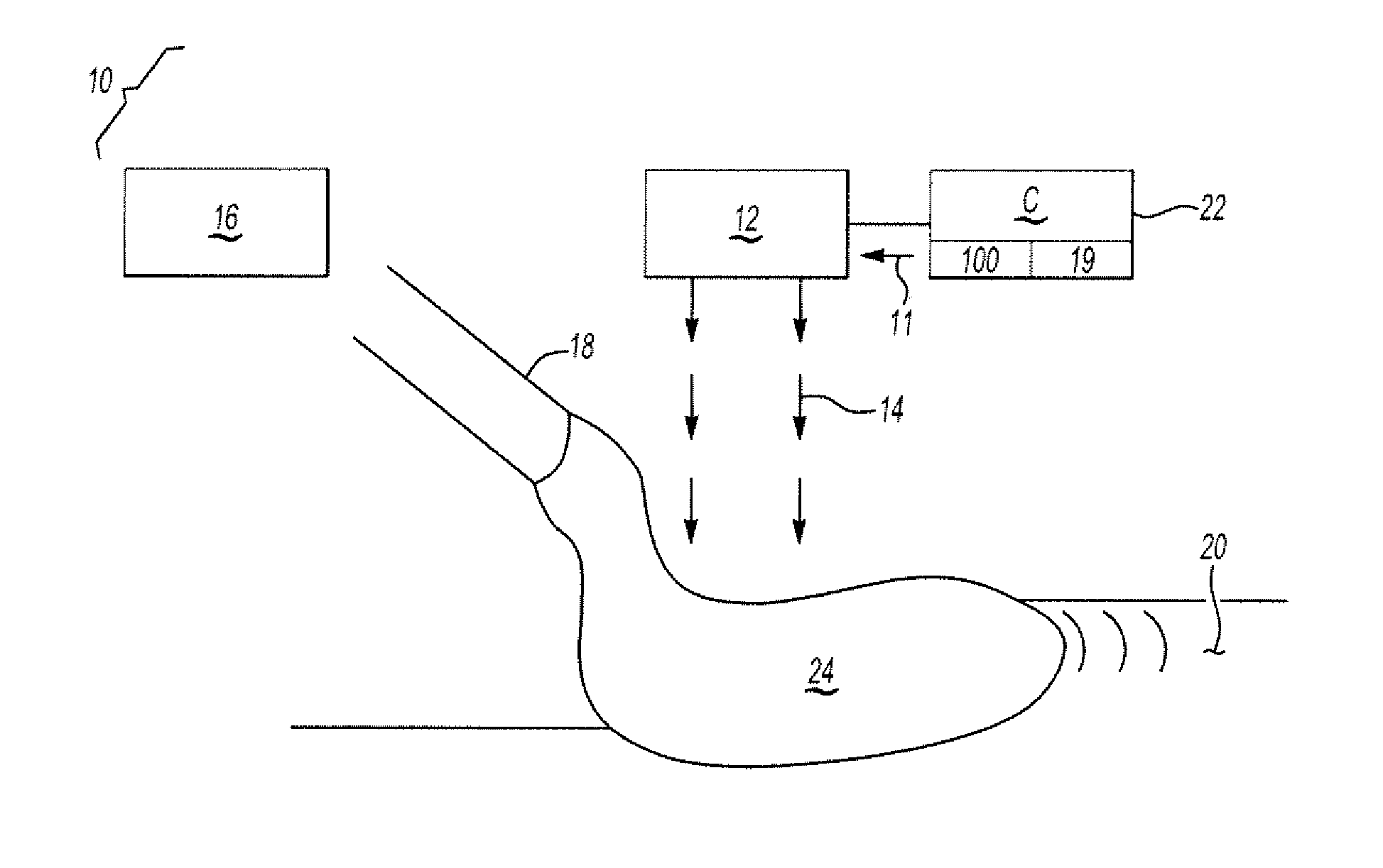
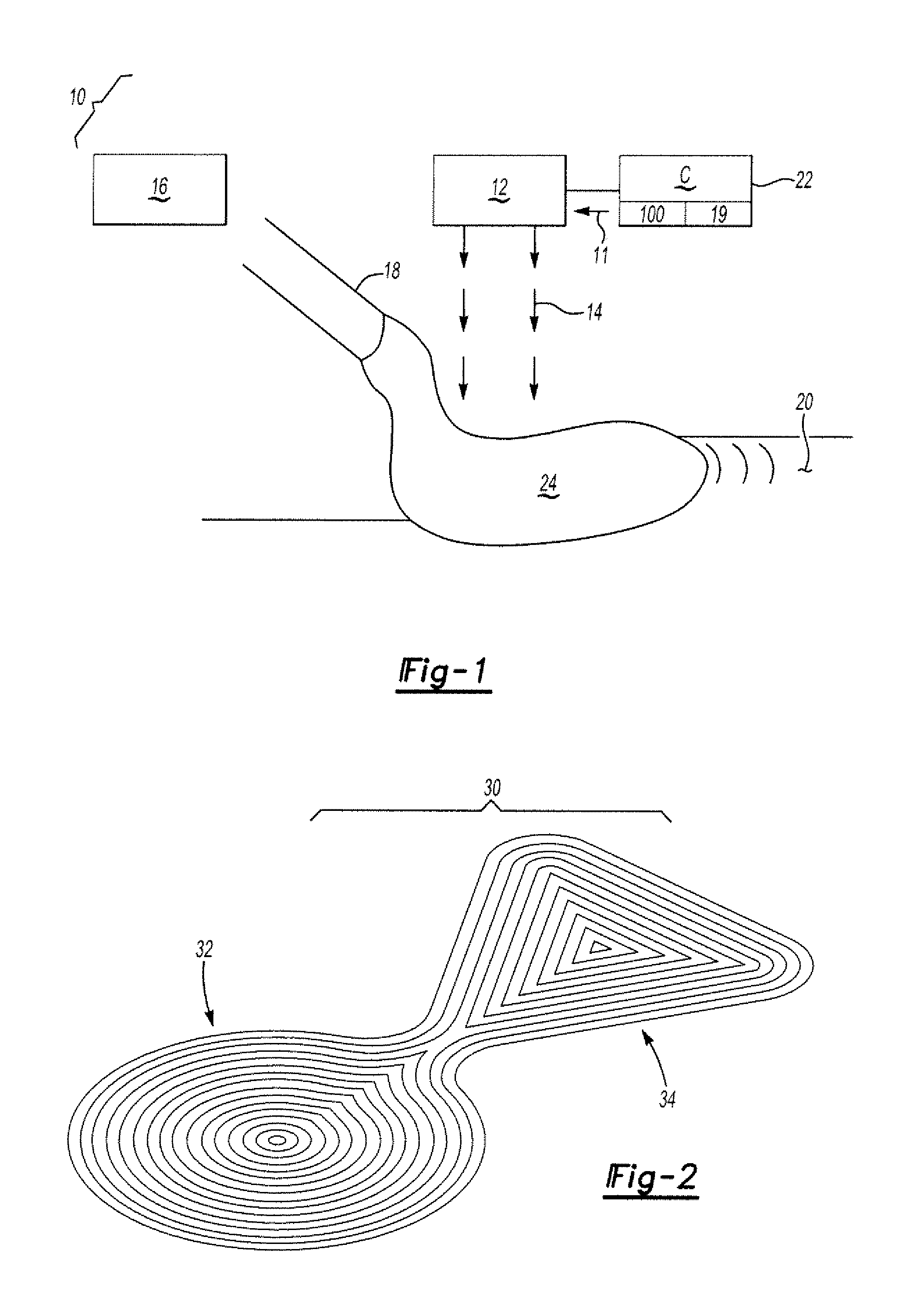
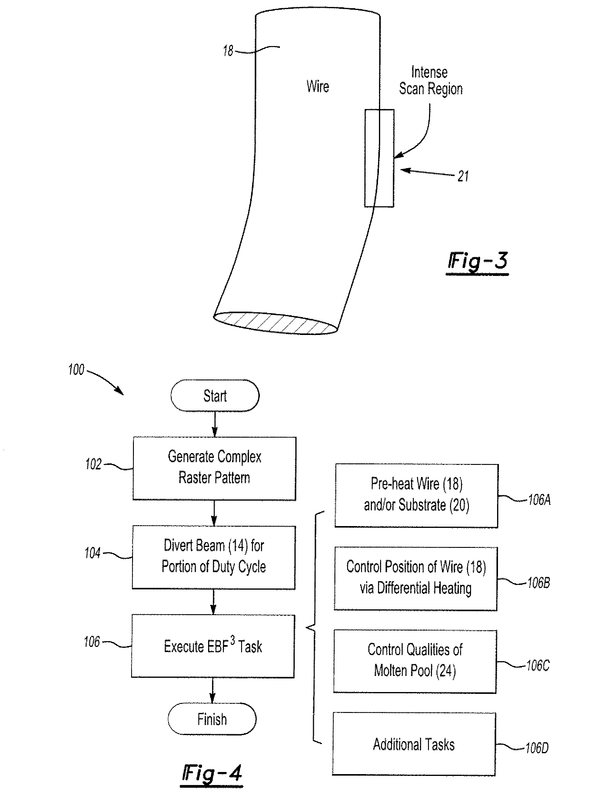
Use of beam deflection to control an electron beam wire deposition process
PatentInactiveUS8344281B2
Innovation
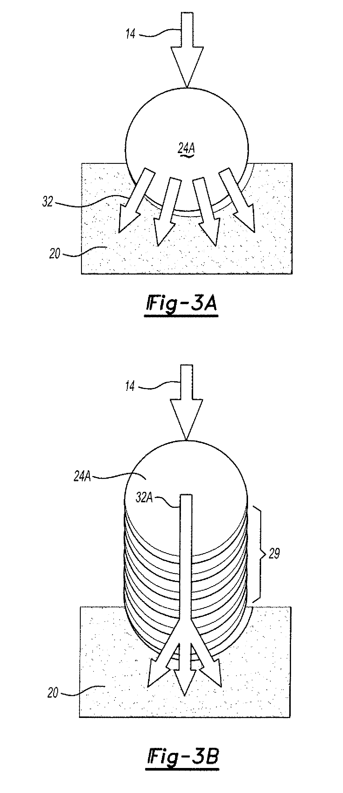
- A method and apparatus that utilize a complex raster pattern for the electron beam to steer and preheat the wire, allowing for simultaneous multi-task processing, self-correction of the wire position, and optimized thermal input, reducing flaws by focusing the beam on the wire's outer edges to maintain it within the molten pool.
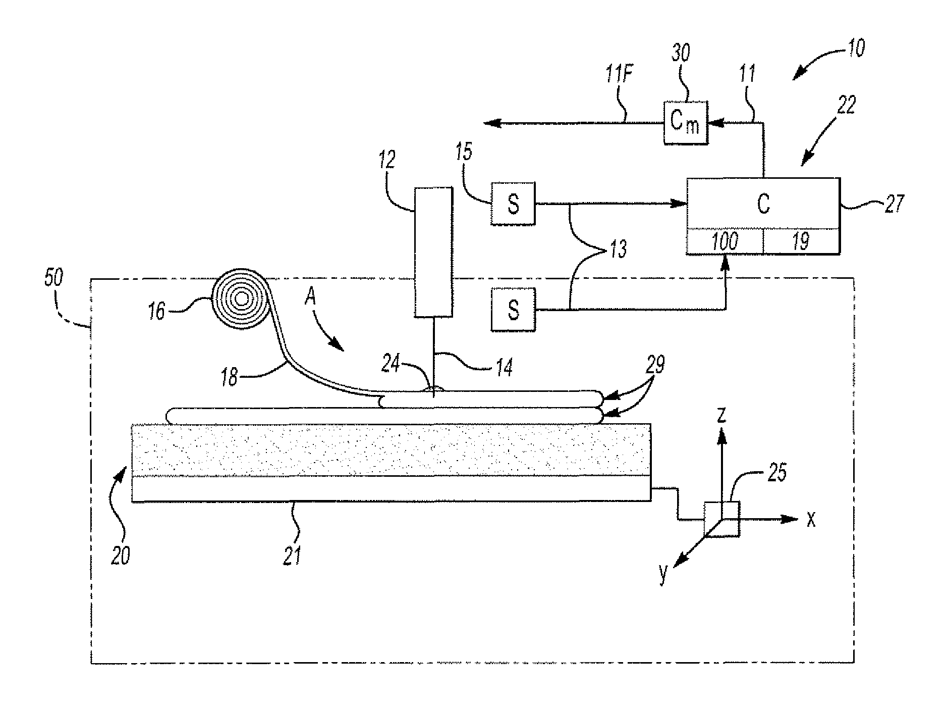
Closed-loop process control for electron beam freeform fabrication and deposition processes
PatentInactiveUS8452073B2
Innovation
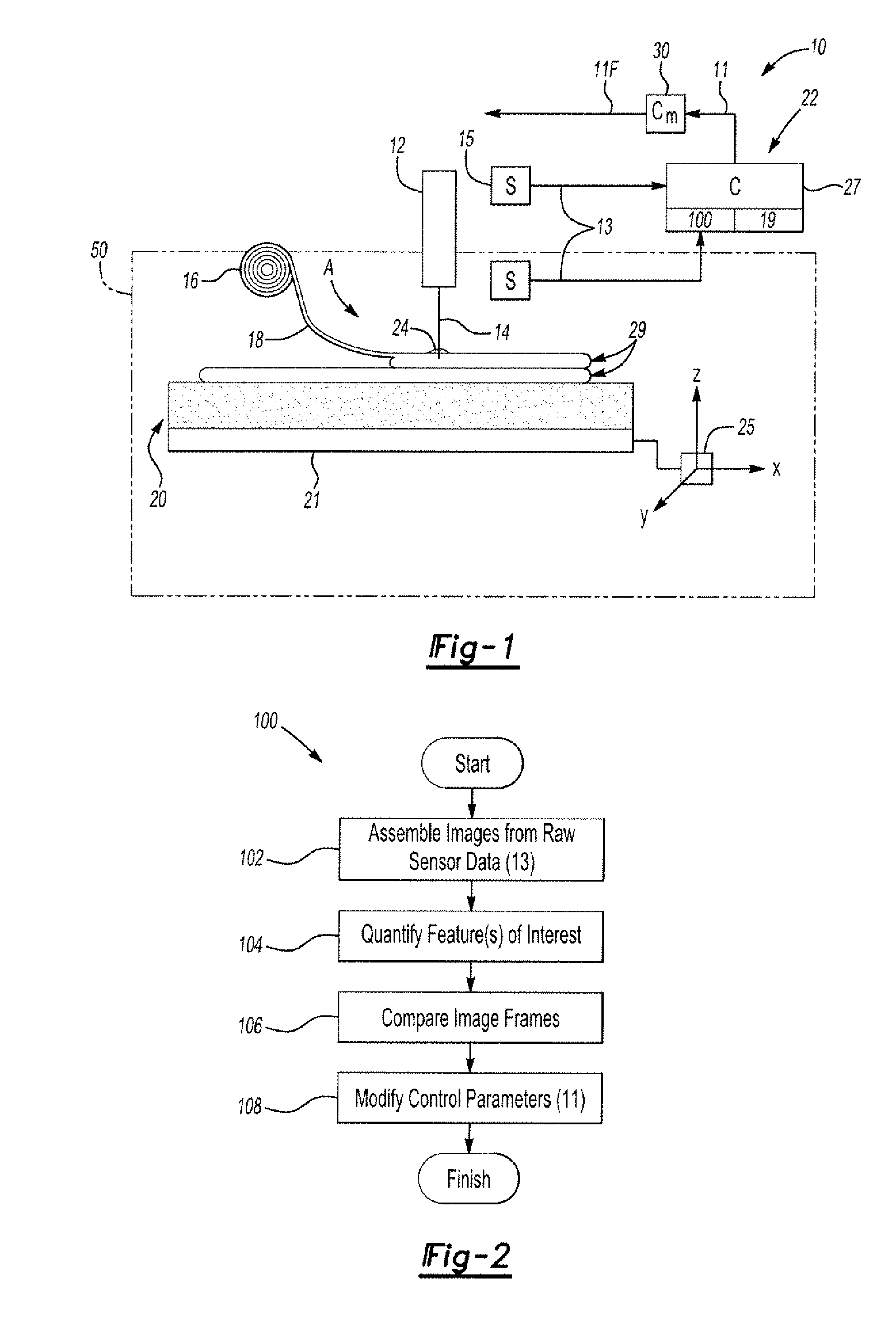
- A closed-loop control method and apparatus that uses sensors to detect features of interest during the EBF3 process, such as the molten pool, and adjusts input parameters in real-time to maintain process consistency, employing an electron gun, wire feeder, host machine, and sensors to continuously evaluate and modify parameters like wire feed rate, beam power, and substrate movement.
Safety Standards and Regulations for Electron Beam Equipment
The regulatory landscape for electron beam equipment encompasses multiple international and national standards designed to ensure operational safety and radiation protection. The International Electrotechnical Commission (IEC) provides foundational standards through IEC 60601 series for medical applications and IEC 62304 for software lifecycle processes in medical devices. These standards establish baseline requirements for equipment design, manufacturing, and testing protocols.
In the United States, the Food and Drug Administration (FDA) regulates electron beam systems through 21 CFR Part 1020, which mandates specific performance standards for electronic products emitting radiation. The Occupational Safety and Health Administration (OSHA) enforces workplace safety requirements under 29 CFR 1910, addressing personnel protection and facility design considerations. Additionally, the Nuclear Regulatory Commission (NRC) oversees certain high-energy electron beam applications through 10 CFR Part 20 radiation protection standards.
European Union regulations follow the Medical Device Regulation (MDR) 2017/745 for medical applications and the Machinery Directive 2006/42/EC for industrial equipment. The European Committee for Electrotechnical Standardization (CENELEC) harmonizes technical standards across member states, ensuring consistent safety requirements. National authorities in individual EU countries may impose additional specific requirements for facility licensing and operator certification.
Key safety parameters mandated by these regulations include maximum allowable radiation leakage rates, typically limited to 0.1% of the useful beam at one meter from the electron path. Interlock systems must meet fail-safe design principles, with redundant safety circuits and emergency shutdown capabilities. Personnel dosimetry requirements mandate continuous monitoring for workers in controlled areas, with annual exposure limits typically set at 20 millisieverts for occupational workers.
Compliance verification involves rigorous testing protocols including commissioning procedures, periodic safety inspections, and performance validation. Equipment manufacturers must demonstrate conformity through third-party testing laboratories and maintain comprehensive documentation throughout the product lifecycle. Regular audits by regulatory bodies ensure ongoing compliance with evolving safety standards and technological advancements in electron beam control systems.
Environmental Impact Assessment of Electron Beam Processing
Electron beam processing presents a compelling environmental profile when compared to conventional manufacturing and sterilization methods. The technology operates without chemical additives, eliminating the need for toxic solvents, catalysts, or sterilizing agents that typically generate hazardous waste streams. This chemical-free approach significantly reduces the environmental burden associated with waste disposal and groundwater contamination risks.
Energy consumption analysis reveals that electron beam systems demonstrate superior efficiency compared to traditional thermal processing methods. The direct energy transfer mechanism achieves processing temperatures instantaneously, eliminating lengthy heating and cooling cycles that characterize conventional ovens and autoclaves. Studies indicate energy savings of 30-50% compared to thermal alternatives, translating to reduced carbon footprint and operational costs.
The atmospheric impact of electron beam processing is notably minimal. Unlike gamma irradiation facilities that require radioactive isotope management, electron beam systems generate radiation only during operation, eliminating long-term radioactive waste concerns. Additionally, the process operates at ambient temperature and pressure, avoiding the release of volatile organic compounds or greenhouse gases typically associated with high-temperature industrial processes.
Water resource conservation represents another significant environmental advantage. Traditional wet chemical processes consume substantial quantities of water for cleaning, rinsing, and waste dilution. Electron beam processing eliminates these requirements entirely, making it particularly valuable in water-scarce regions and contributing to sustainable manufacturing practices.
Waste stream reduction constitutes a primary environmental benefit. The precision control inherent in electron beam systems minimizes material degradation and processing rejects, leading to higher yield rates and reduced raw material consumption. The absence of chemical residues eliminates the need for post-processing cleaning steps, further reducing waste generation and associated environmental impacts.
Life cycle assessments consistently demonstrate favorable environmental profiles for electron beam processing across multiple application sectors, including food preservation, medical device sterilization, and polymer modification, positioning the technology as an environmentally sustainable alternative to conventional processing methods.
Unlock deeper insights with PatSnap Eureka Quick Research — get a full tech report to explore trends and direct your research. Try now!
Generate Your Research Report Instantly with AI Agent
Supercharge your innovation with PatSnap Eureka AI Agent Platform!