
A kind of tungsten-copper alloy surface nanometerization method
A tungsten-copper alloy and nanotechnology, which is applied in the field of material surface treatment, can solve problems such as partial surface melting and material failure, and achieve the effects of reduced cut-off value, low cost, and simple operation
Patent Information
- Authority / Receiving Office
- CN · China
- Patent Type
- Patents(China)
- Current Assignee / Owner
- Publication Date
- 2016-04-06
Smart Images
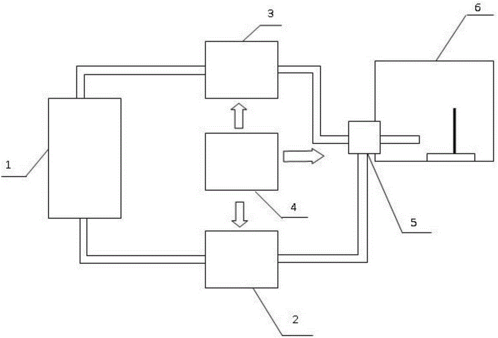
Figure 1 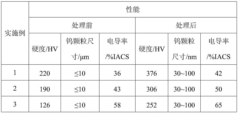
Figure 2
Abstract
Description
technical field
[0001] The invention belongs to the technical field of material surface treatment, and relates to a method for nanometerizing the surface of a tungsten-copper alloy. Background technique
[0002] Tungsten-copper alloy has the properties of high temperature resistance, arc ablation resistance, fusion welding resistance, small cut-off current, low thermal electron emission ability, etc., and is widely used in electrical contact materials and high temperature resistant parts in aerospace. Although tungsten copper alloy has been widely used, its performance still needs to be improved. When tungsten-copper alloy is used as an electrical contact material in service, the strong arc generated by high voltage and high current during the switching process gathers on the surface of the material, resulting in severe local melting on the surface, forming ablation pits and causing premature failure of the material. Studies have found that the performance of tungsten-coppe...
Examples
Embodiment 1
[0028] Step 1, mechanically polishing the surface of the tungsten-copper alloy with a copper content of 20% and cleaning the surface oil with acetone;
[0029] Step 2, place the tungsten-copper alloy pretreated in step 1 in a supersonic particle bombardment device for surface nano-treatment; the process parameters are: gas (air) pressure of 3.5MPa, hard particle size of 0.3mm, hard The particle flow rate is 25g / s, the hard particles are S110 stainless steel, the voltage is 30V, and the processing time is 10min;
[0030] Step 3, place the tungsten-copper alloy that has been treated with surface nanometerization in step 2 in a vacuum furnace, and the vacuum degree is 1×10 -3 Pa, annealing temperature 200°C, and annealing time 30 minutes can be used for stress relief annealing.
[0031] The thickness of the nano-layer on the surface of the tungsten-copper alloy obtained in Example 1 is 0.45 mm.
Embodiment 2
[0033] Step 1, mechanically polishing the surface of a tungsten-copper alloy with a copper content of 30% and cleaning the surface with acetone to remove oil stains;
[0034] Step 2, place the tungsten-copper alloy pretreated in step 1 in a supersonic particle bombardment device for surface nano-treatment; the process parameters are: gas (nitrogen) pressure 2.5MPa, hard particle size 0.3mm, hard The particle flow rate is 20g / s, the hard particles are S110 stainless steel, the voltage is 20V, and the processing time is 60min;
[0035] Step 3, place the tungsten-copper alloy that has been treated with surface nanometerization in step 2 in a vacuum furnace, and the vacuum degree is 1×10 -3 Pa, annealing temperature 200°C, and annealing time 30 minutes can be used for stress relief annealing.
[0036] The thickness of the nano-layer on the surface of the tungsten-copper alloy obtained in Example 2 is 0.8 mm.
Embodiment 3
[0038] Step 1, mechanically polish the surface of the tungsten-copper alloy with a copper content of 50% and clean the surface oil with alcohol;
[0039] Step 2, place the tungsten-copper alloy pretreated in step 1 in a supersonic particle bombardment device for surface nano-treatment; the process parameters are: gas (air) pressure 1.5MPa, hard particle size 0.3mm, hard particle The flow rate is 15g / s, and the hard particles are α-Al 2 o 3 , voltage 20V, processing time 45min;
[0040] Step 3, place the tungsten-copper alloy that has been treated with surface nanometerization in step 2 in a vacuum furnace, and the vacuum degree is 1×10 -3 Pa, annealing temperature 200°C, and annealing time 30 minutes can be used for stress relief annealing.
[0041] The thickness of the nano-layer on the surface of the tungsten-copper alloy obtained in Example 3 is 1.1 mm.