
Method of Inducing Quantum Well Mixing Using Laser Micro-region Plasma
A laser plasma and plasma technology, applied in the manufacture of semiconductor/solid-state devices, electrical components, circuits, etc., can solve the problems of increasing light absorption rate and changing the width of the band gap, saving time, easy area selection operation, and realizing The effect of large-scale industrialization
Patent Information
- Authority / Receiving Office
- CN · China
- Patent Type
- Patents(China)
- Current Assignee / Owner
- Publication Date
- 2016-04-27
Smart Images
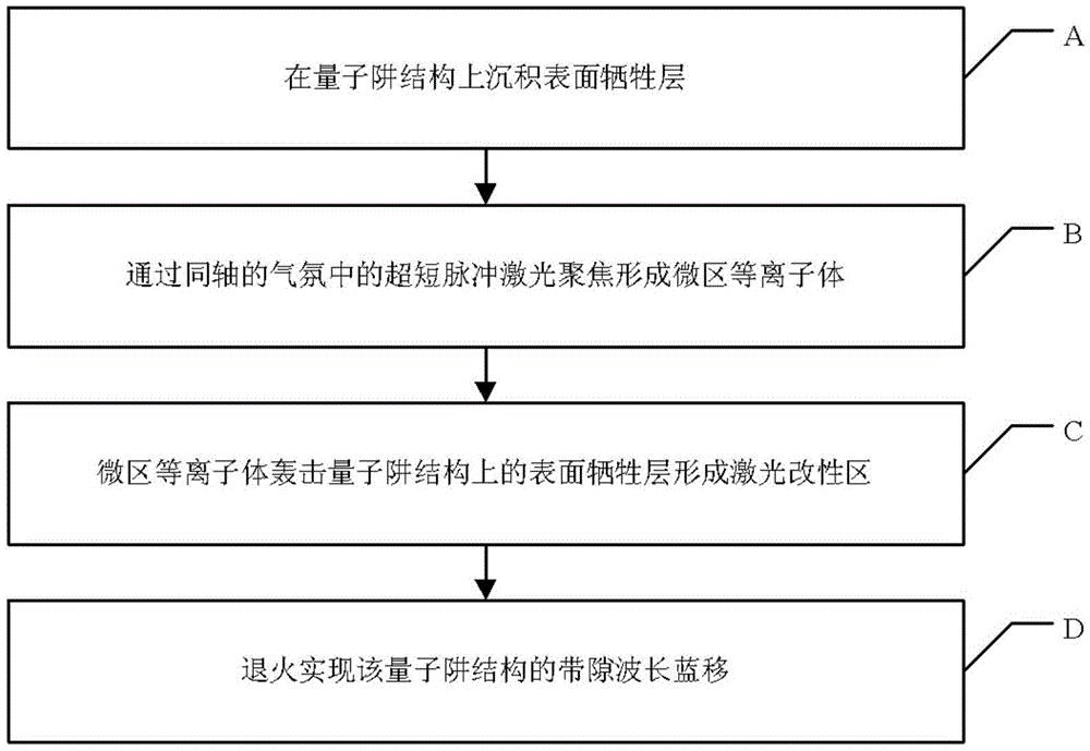
Figure 1
Abstract
Description
technical field
[0001] The invention relates to semiconductor optical device and photonic integrated circuit technology, in particular to a method for using laser micro-region plasma to induce quantum well mixing. Background technique
[0002] Photonic integration is to integrate dozens or even hundreds of optical components into a single integrated circuit or chip. Since it is very difficult to integrate various optical devices on one chip, the commercialization of photonic integrated circuits is very difficult. slow. The biggest difference from microelectronic integrated circuits based on silicon materials, monolithic photonic integrated circuits are currently mainly based on indium phosphide gallium arsenic material systems, and various materials with different photonic band gaps need to be formed on the same substrate to meet various requirements. The requirements of active and passive devices, such as detectors in optical integrated circuits need to absorb light, while...
Examples
Embodiment Construction
[0015] see figure 1 As shown, the present invention provides a kind of method utilizing laser micro-region plasma to induce quantum well mixing, comprising the following steps:
[0016] Step A: Deposit a surface sacrificial layer on the quantum well layer on the quantum well structure sheet, the thickness of the surface sacrificial layer is 50nm-500nm, and its material is indium phosphide, indium gallium arsenic, indium gallium arsenic phosphide, aluminum gallium arsenic, dioxide Silicon or silicon nitride, the quantum well layer is a single quantum well structure or multiple quantum well structure, the quantum well layer is InGaAs / InGaAsP, AlGaAs / GaAs, AlGaAs / InGaAs or AlGaInP / GaAs;
[0017] Step B: The laser beam is focused on the sacrificial layer on the surface through a laser head with a gas supply function to form a laser plasma of a reaction gas. The gas supply function is usually a coaxial gas supply with a nozzle, which can control the gas flow, pressure and speed; ...