
Avalanche photodetector based on arc-shaped diffusion region and its manufacturing method
An avalanche photoelectric and diffusion area technology, applied in circuits, electrical components, semiconductor devices, etc., can solve the problems of reduced detection efficiency of single-photon detectors, increased detection efficiency of devices, and decreased overall device performance, so as to improve photon detection efficiency, Reduce the probability of post-pulse and reduce the effect of edge electric field
Patent Information
- Authority / Receiving Office
- CN · China
- Patent Type
- Patents(China)
- Current Assignee / Owner
- Publication Date
- 2020-06-19
Smart Images
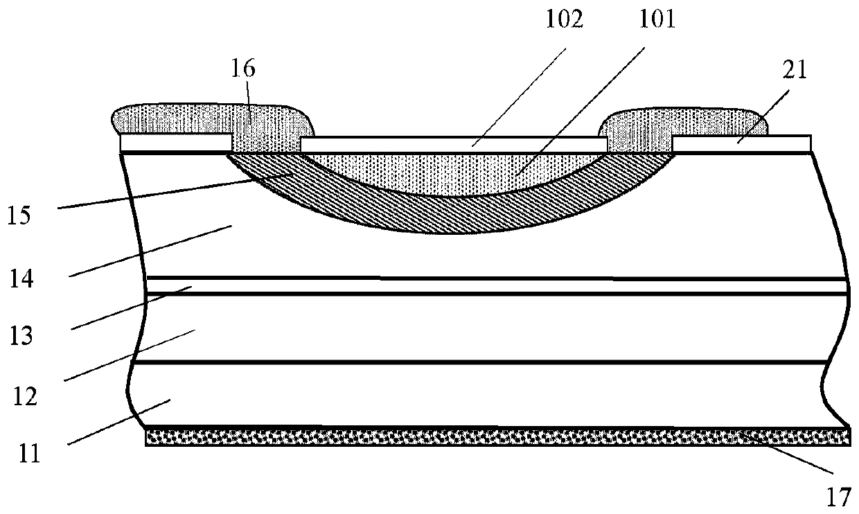
Figure 1 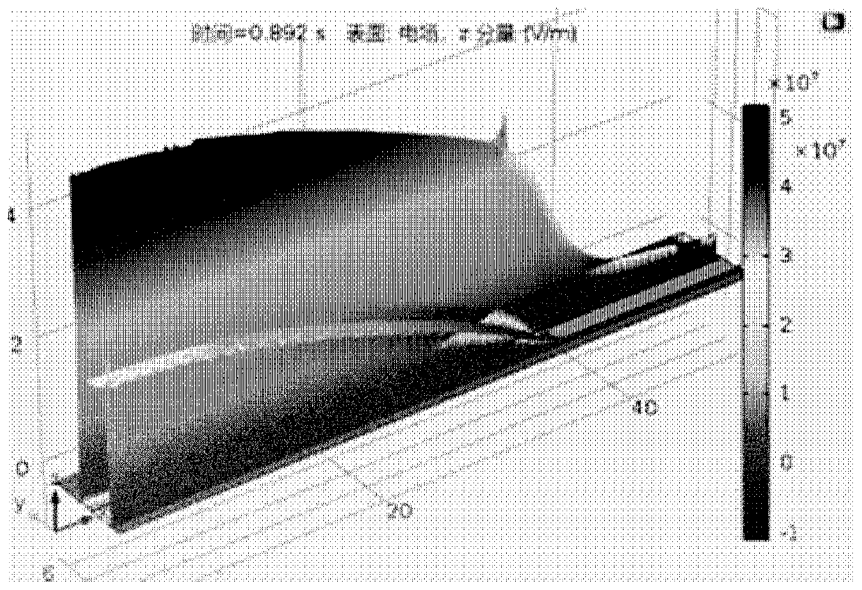
Figure 2 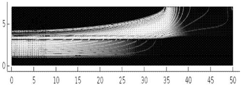
Figure 3
Abstract
Description
technical field
[0001] The disclosure belongs to the technical field of semiconductor devices, and relates to an avalanche photodetector based on an arc-shaped diffusion region and a manufacturing method thereof. Background technique
[0002] Avalanche photodetectors (APD, Avalanche Photo-Detector) have been widely used in commercial, military and scientific research, such as quantum information, biomolecular detection, lidar imaging and astronomical detection. The single-photon APD with high speed in the communication band, high detection efficiency, and low number of secrets has played an extremely important role in the actual quantum key distribution system. Single Photon Avalanche Photodetector (SPAD, Single Photon Avalanche-Detector) Due to its special Geiger working method, the avalanche process and avalanche current density have a great influence on the detection efficiency and dark count of the device. The detection efficiency of the photon is low, and the high dete...
Examples
Embodiment Construction
[0032] The disclosure provides an avalanche photodetector based on an arc-shaped diffusion region and its manufacturing method. By forming a 3D bowl-shaped opening in the intrinsic multiplication layer and performing high P-type doping in the bowl-shaped opening, the center of the window The partially undiffused multiplication layer has the smallest thickness, and the edge thickness is the largest, so as to form a P-type highly doped arc-shaped diffusion region, so that the central part of the light field in the multiplication region of the avalanche detector has the strongest gain, and the impact ionization of the multiplication region is more uniform in the lateral direction , reduce the edge electric field and the resulting edge breakdown, and ensure the spatial coincidence of the center light field and the strongest electric field of the device, which can effectively improve the photon detection efficiency of the device, reduce the dark count of the device, and reduce the po...