
Sensor for coordinate input device
a technology of input device and sensor, which is applied in the direction of static indicating device, using reradiation, instruments, etc., can solve the problems reducing the invalid area, increasing the detectable area, etc., and reducing the overall size of the sensor. , the effect of reducing the overall size of the sensor
Patent Information
- Authority / Receiving Office
- US · United States
- Patent Type
- Applications(United States)
- Current Assignee / Owner
- Publication Date
- 2005-06-23
Smart Images
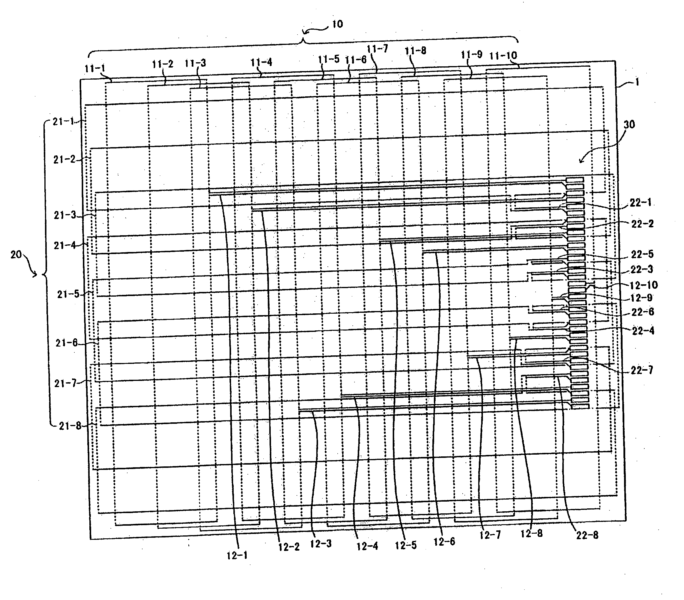
Figure 1 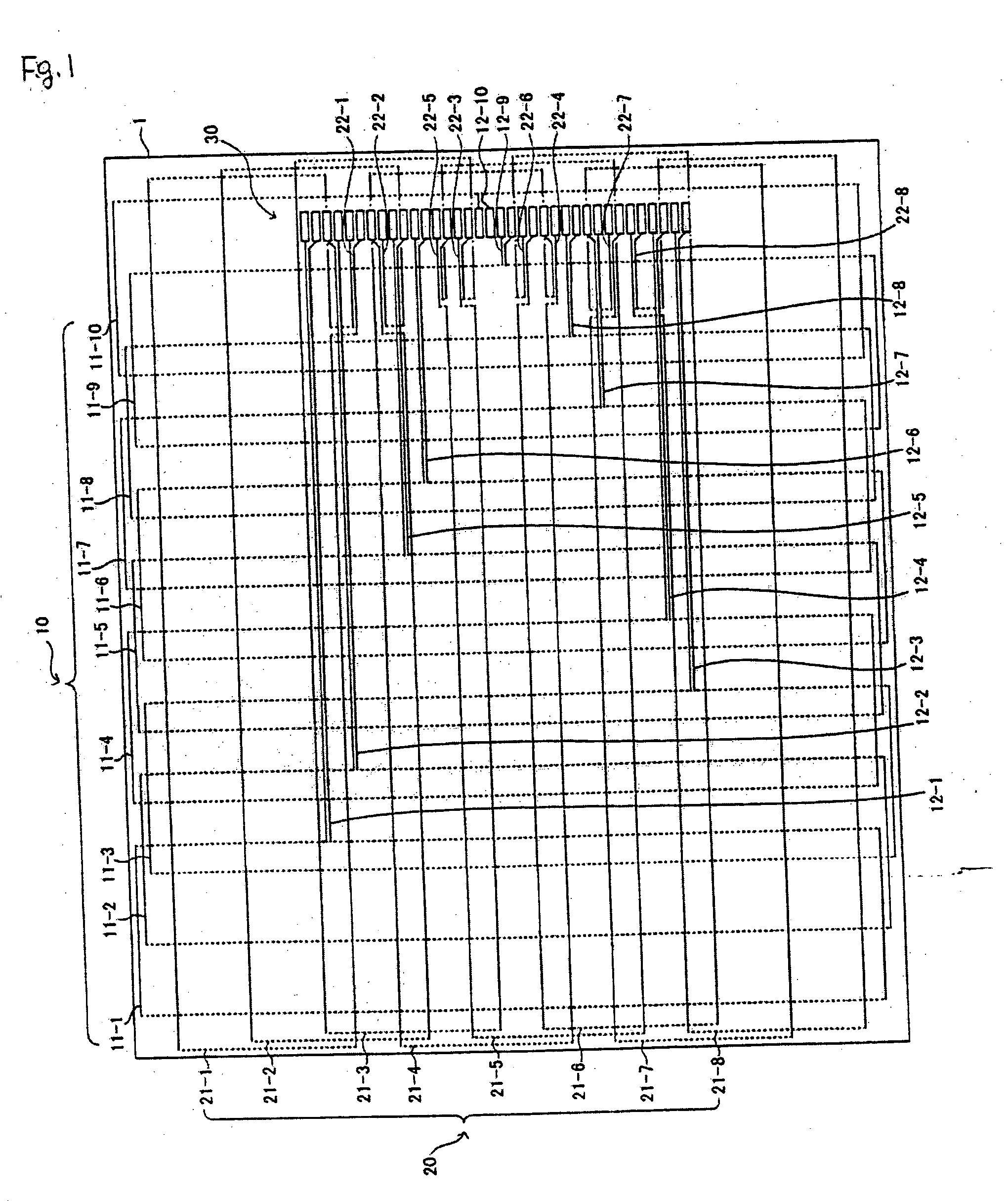
Figure 2 
Figure 3
Abstract
Description
CROSS-REFERENCE TO RELATED APPLICATIONS AND CLAIM TO PRIORITY
[0001] This application claims the benefit under 35 U.S.C. § 119 of application number 2003-400370, filed Nov. 28, 2003 in Japan, the disclosure of which is incorporated herein by reference.
[0002] 1. Field of the Invention
[0003] The present invention relates to a sensor for a coordinate input device using an electromagnetic effect.
[0004] 2. Background of the Invention
[0005] Conventional coordinate input devices are well known in the prior art. These devices use a sensor that has a large number of loop coils arranged in x and y directions and a position indicator that includes a coil. In these coordinate input devices, a sensor detects a position indicated by the position indicator using an electromagnetic effect between the sensor and the position indicator.
[0006] The sensor used by the coordinate input device must have lines for supplying power to the respective loop coils and for extracting signals from the loop co...
Examples
Embodiment Construction
)
[0033] An embodiment of the present invention will be described below with reference to the accompanying drawings.
[0034]FIG. 1 is a plan view showing the configuration of a sensor 1 for a coordinate input device according to an embodiment of the present invention. In FIG. 1, reference numeral 10 indicates an x-direction loop coil group and reference numeral 20 indicates a y-direction loop coil group.
[0035] The sensor 1 includes, for example, a rigid substrate, such as a glass epoxy substrate. The solid lines and the dotted lines shown in FIG. 1 indicate wires provided on the substrate. The substrate of the sensor 1 has a plurality of layers and the wires indicated by the solid lines and dotted lines in FIG. 1 are provided by patterns in different layers. Both of the wires indicated by the solid lines and the wires indicated by the dotted lines in FIG. 1 are coated with insulating films and are not exposed at a surface of the sensor 1.
[0036] A shield plate 13 (see FIG. 4) is lami...