
Semiconductor device and method for manufacturing the same
a technology of semiconductors and semiconductors, applied in the direction of inductances, galvano-magnetic devices, basic electric elements, etc., can solve the problems of significant influence of parasitic capacitance, energy loss, and part of electromagnetic energy generated by induction elements in the substrate, and achieve low energy-loss and high performance.
Patent Information
- Authority / Receiving Office
- US · United States
- Current Assignee / Owner
- Publication Date
- 2006-02-02
- Estimated Expiration
- Not applicable · inactive patent
Smart Images
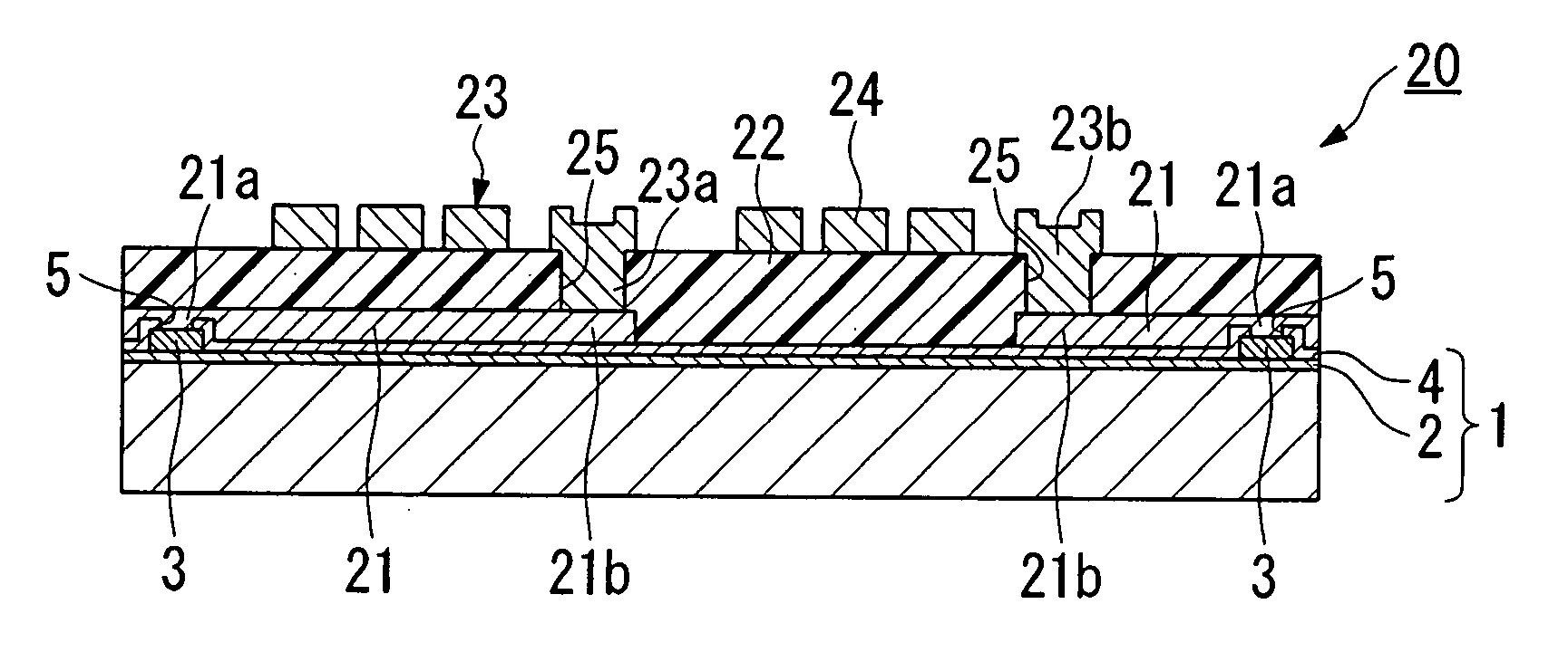
Figure 1 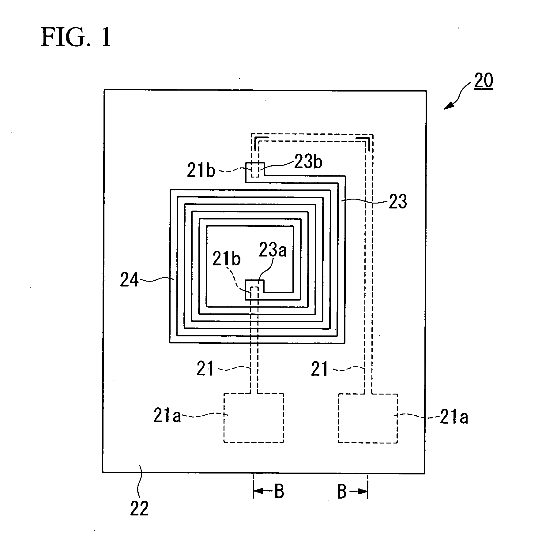
Figure 2 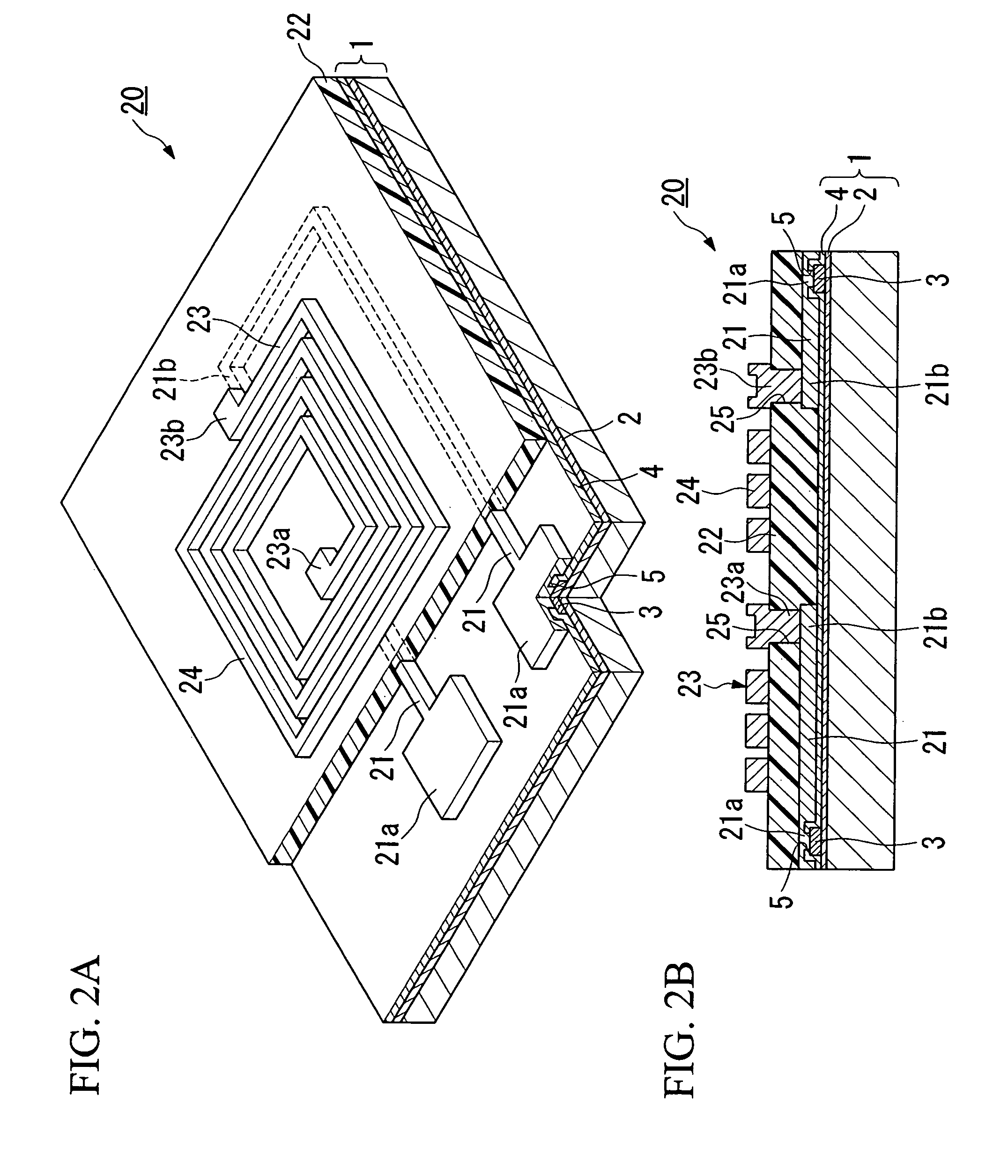
Figure 3
Abstract
Description
BACKGROUND OF THE INVENTION
[0001] 1. Field of the Invention
[0002] The present invention relates to a semiconductor device and a method for manufacturing the same in which formation of a semiconductor having a induction element formed above a semiconductor substrate, such as a silicon wafer is done together with packaging thereof.
[0003] Priority is claimed on Japanese Patent Application No. 2004-221785, filed Jul. 29, 2004, and Japanese Patent Application No. 2004-302696, filed Oct. 18, 2004, the contents of which are incorporated herein by reference.
[0004] 2. Description of Related Art
[0005] In recent years, in a fabrication of a high-frequency semiconductor element, an induction element, such as a spiral inductor, is formed on a semiconductor substrate for the purpose of ensuring impedance matching thereof or the like. In such a semiconductor element, however, a part of electromagnetic energy generated by the induction element is lost in the substrate or a wiring constructing ...