
Metal electroplating process of an electrically connecting pad structure of circuit board and structure thereof
a technology of which is applied in the direction of resist details, patterning and lithography, and non-metallic protective coating applications. it can solve the problems of ineffective cutting of electrical connection between electrically connecting pads and electroplating lines, adverse effects on electrical performance of circuit boards, and product yield, so as to effectively prevent the permeation of electroplating materials, reduce the thickness of stencils and circuit layers, and easy to remove
Patent Information
- Authority / Receiving Office
- US · United States
- Patent Type
- Applications(United States)
- Current Assignee / Owner
- Publication Date
- 2006-12-07
- Estimated Expiration
- Not applicable · inactive patent
Smart Images
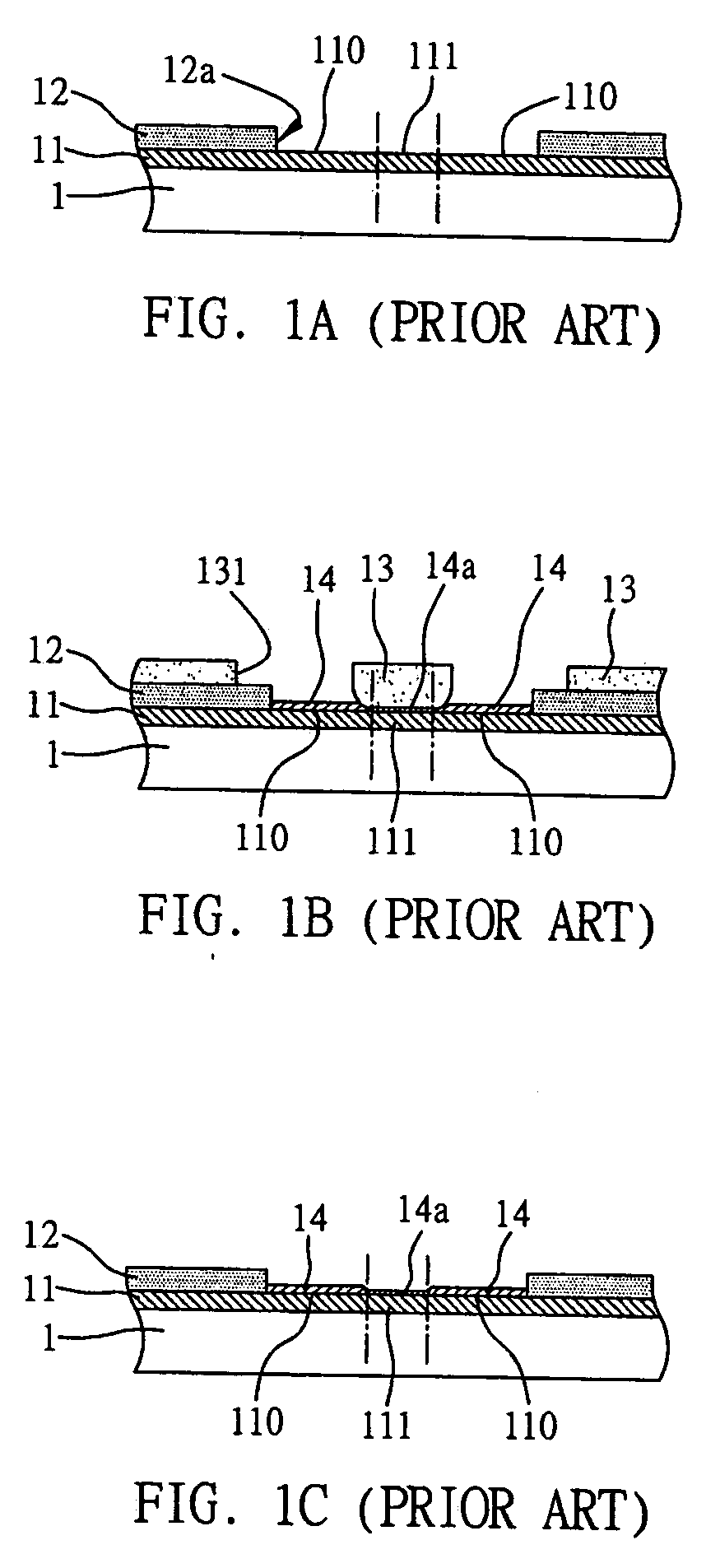
Figure 1 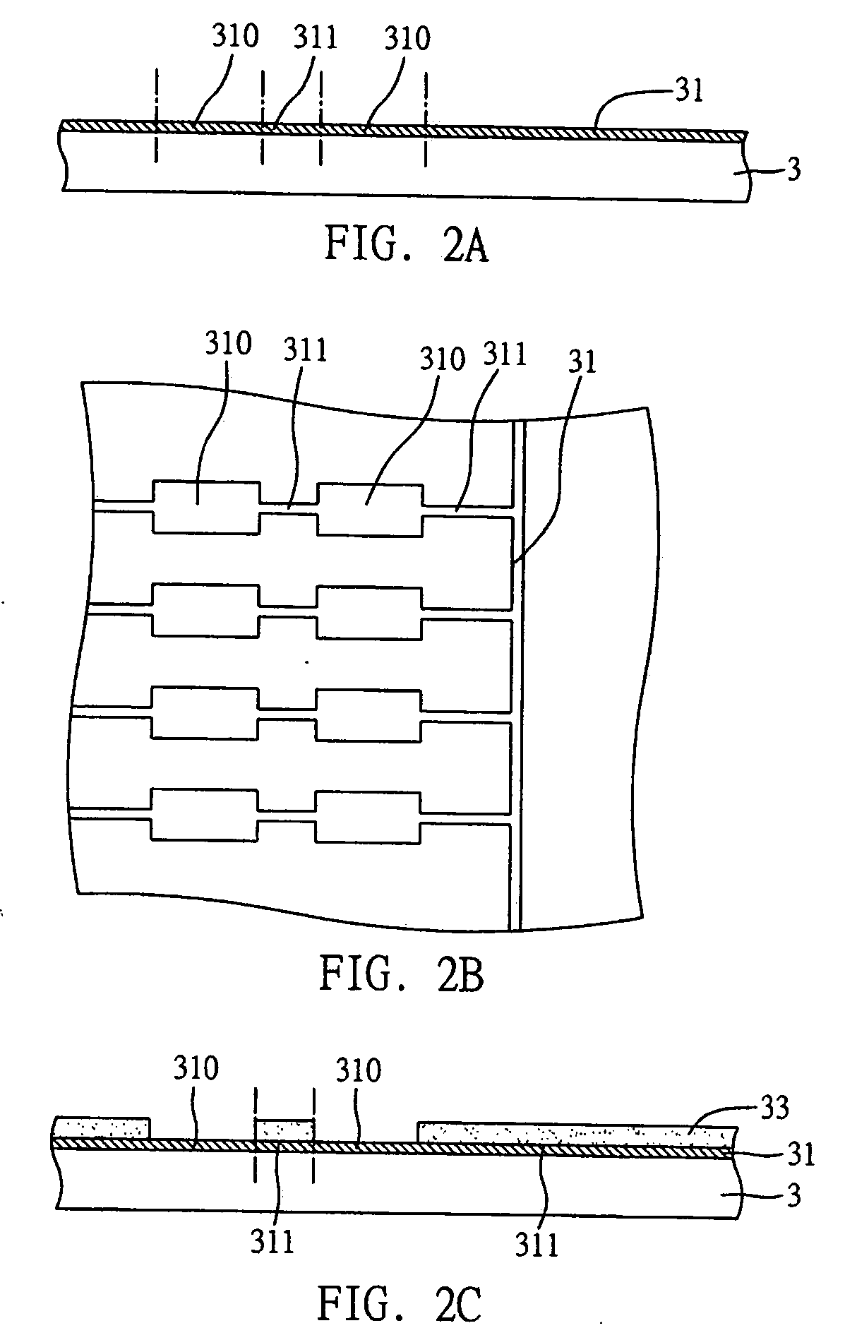
Figure 2 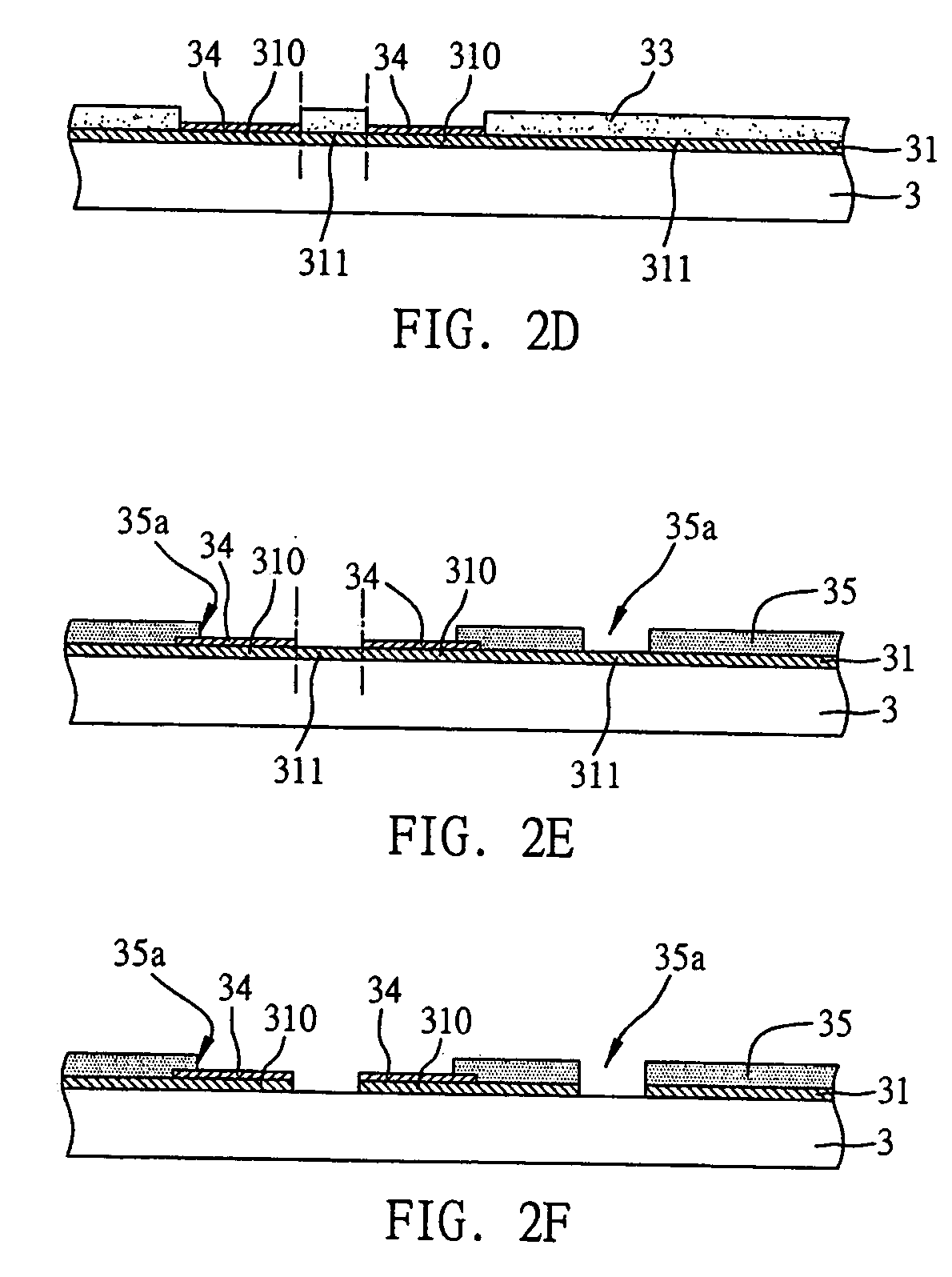
Figure 3
Abstract
Description
CROSS-REFERENCE TO RELATED APPLICATIONS
[0001] This application claims benefit under 35 USC 119 of Taiwan Application No. 094118704, filed Jun. 7, 2005. FIELD OF THE INVENTION
[0002] The present invention relates to a metal electroplating process of an electrically connecting pad structure of circuit boards, and more particularly to electroplating a Ni / Au layer on exposed surface of electrically connecting pads of circuit boards. BACKGROUND OF THE INVENTION
[0003] In general, a circuit board comprises a plurality of conductive circuits made of such as copper. For electronic signal transmission or power signal transmission, a plurality of electrically connecting pads is extended from the conductive circuits. Furthermore, a Ni / Au layer can be formed on the exposed surface of the electrically connecting pads such that conductive components such as gold wires and solder balls can effectively be coupled to the electrically connecting pads through the Ni / Au layer. In addition, the Ni / Au l...
Examples
Embodiment Construction
[0014] Hereunder, embodiments of the present invention will be described in full detail with reference to the accompanying drawings.
[0015]FIGS. 2A to 2F are sectional diagrams showing a metal electroplating process of an electrically connecting pad structure of a circuit board according to the present invention.
[0016] Referring to FIGS. 2A and 2B, a circuit board 3 with a patterned circuit layer 31 formed on at least one surface thereof is provided. The circuit layer 31 defines a plurality of electrically connecting pads 310 and electroplating lines 311 connected to the electrically connecting pads 310. The circuit layer 31 can be made of Cu.
[0017] Referring to FIG. 2C, a patterned resist layer 33 is formed on the circuit layer 31 of the circuit board 3 with the electroplating lines 311 being covered by the patterned resist layer 33 and the electrically connecting pads 310 being exposed from the patterned resist layer 33. The resist layer 33 can be deposited on the circuit layer ...