
Coreless packaging substrate and method of fabricating the same
a packaging substrate and coreless technology, applied in the direction of semiconductor devices, electrical equipment, semiconductor/solid-state device details, etc., can solve the problems of increasing the thickness of the overall structure, increasing the difficulty of the process, weakening the bonding force, etc., to achieve the effect of reducing the distance between metal bumps, simple manufacturing of packaging substrates, and not prone to falling off and being damaged
Patent Information
- Authority / Receiving Office
- US · United States
- Patent Type
- Applications(United States)
- Current Assignee / Owner
- Publication Date
- 2016-04-21
Smart Images
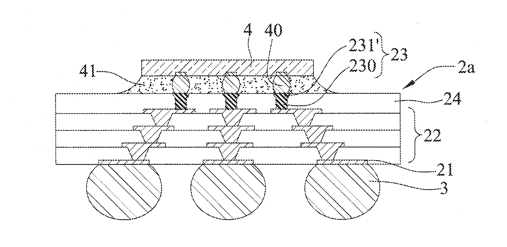
Figure 1 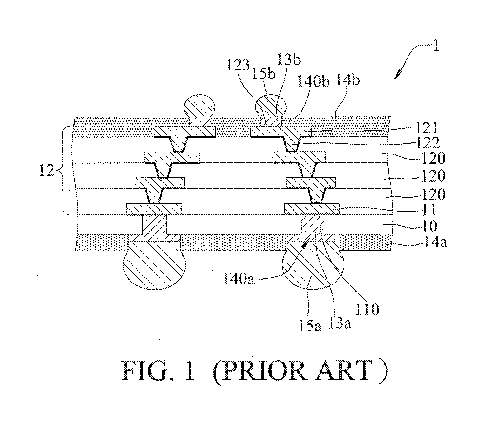
Figure 2 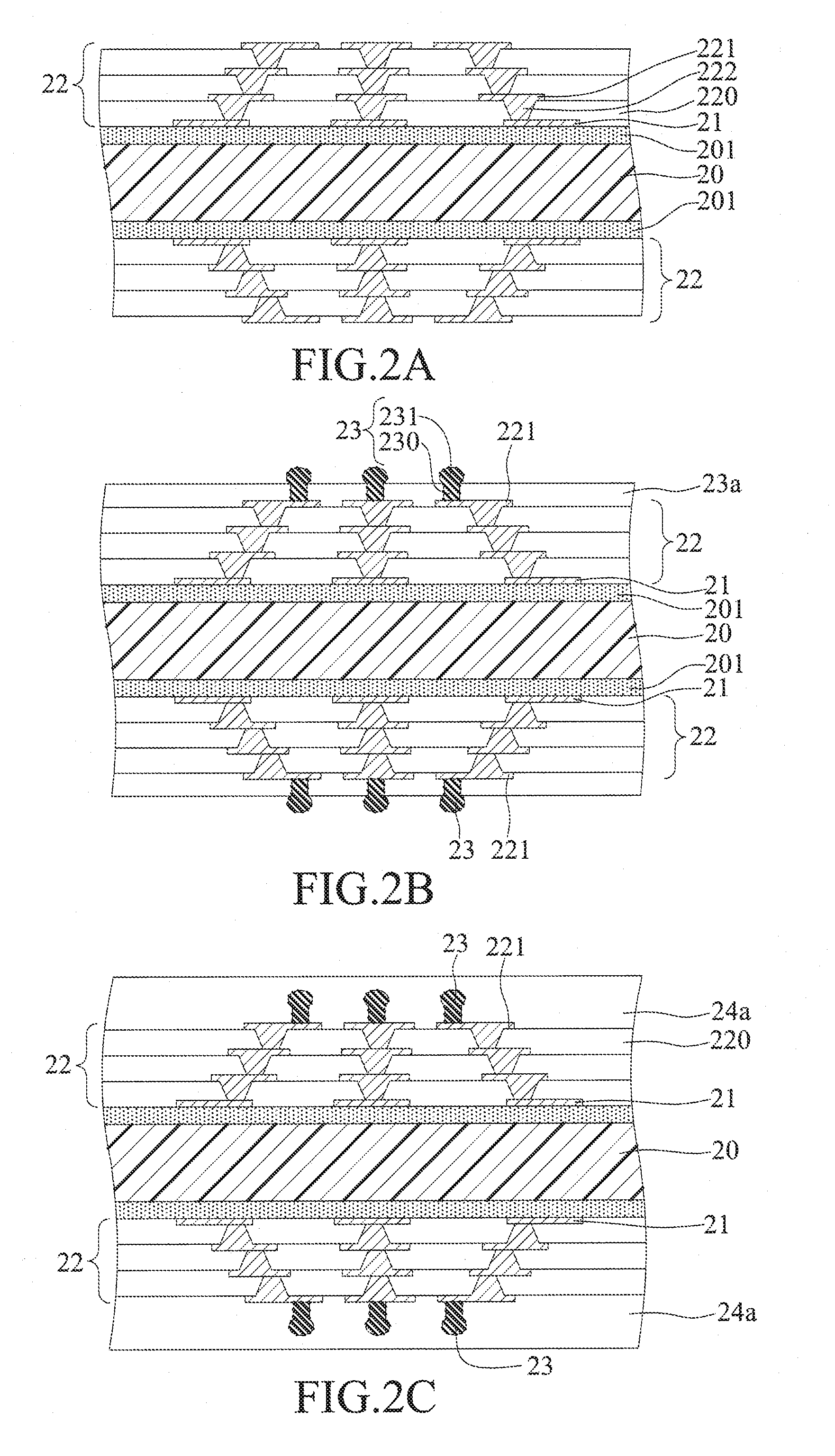
Figure 3
Abstract
Description
RELATED APPLICATIONS
[0001] The present application is a Divisional application of U.S. application Ser. No. 13 / 417,858, filed on Mar. 12, 2012, which claims priority of Taiwan Application Serial Number 100124353, filed on Jul. 8, 2011, all of which are herein incorporated by reference.BACKGROUND
[0002] 1. Technical Field
[0003] The present invention relates generally to packaging substrates, and, more particularly, to a coreless packaging substrate and a method of fabricating the same.
[0004] 2. Description of Related Art
[0005] With the rapid development of electronic industry, electronic products are trending toward multi-function and high-performance. Currently, the semiconductor package structure has developed various package types such as wire bonding or flip chip that forms a semiconductor chip on a packaging substrate, and the semiconductor chip electrically connects to the packaging substrate by bonding wires or solder bumps. In order to meet the packaging requirements of high integr...
Examples
Embodiment Construction
[0021]It is to be understood that both the foregoing general descriptions and the following detailed embodiments are exemplary and are, together with the accompanying drawings, intended only to provide further explanation of technical features and advantages of the invention.
[0022]The following illustrative embodiments are provided to illustrate the disclosure of the present invention, these and other advantages and effects can be apparent to those skilled in the art after reading the disclosure of this specification. The present invention can also be performed or applied by other different embodiments. The details of the specification may be on the basis of different points and applications, and numerous modifications and variations can be devised without departing from the spirit of the present invention.
[0023]FIGS. 2A to 2E are schematic cross-sectional views illustrating a method of fabricating a coreless packaging substrate according to the present invention.
[0024]As shown in F...