
Sgvc 3D architecture with floating gate device in lateral recesses on sides of conductive strips and insulating strips
Patent Information
- Authority / Receiving Office
- US · United States
- Current Assignee / Owner
- Publication Date
- 2017-07-06
Smart Images
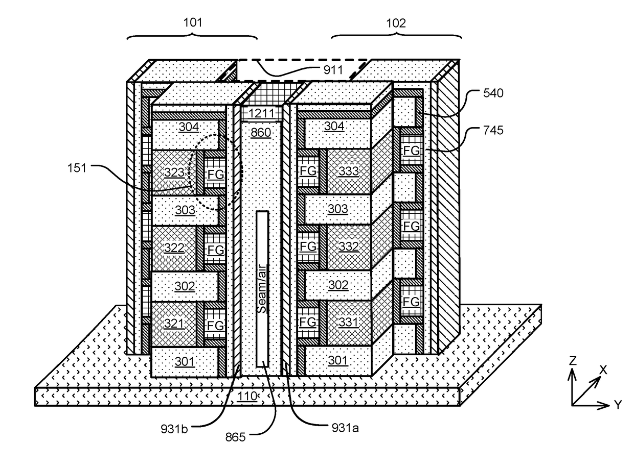
Figure 1 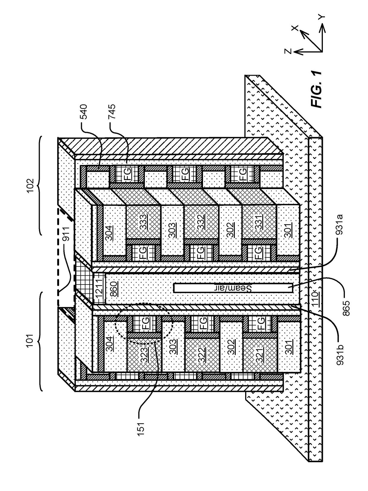
Figure 2 
Figure 3
Abstract
Description
PRIORITY APPLICATION
[0001] This application claims priority to Taiwan Patent Application No. 104144348, filed 30 Dec. 2015, which application is incorporated by reference as if fully set forth herein.RELATED APPLICATIONS
[0002] This application is related to co-pending U.S. patent application Ser. No. 14 / 637,204, filed 3 Mar. 2015, entitled U-SHAPED VERTICAL THIN-CHANNEL MEMORY (Attorney Docket No. 2147-1B), which application is incorporated by reference as if fully set forth herein.BACKGROUND
[0003] Field of the Technology
[0004] The present invention relates to high density memory devices, and particularly to memory devices in which multiple planes of memory cells are arranged to provide a three-dimensional 3D array.
[0005] Description of Related Art
[0006] High density memory devices are being designed that comprise arrays of flash memory cells, or other types of memory cells. In some examples, the memory cells comprise thin film transistors which can be arranged in 3D architectures.
[0007] I...
Examples
Embodiment Construction
[0034]A detailed description of embodiments of the present technology is provided with reference to the Figures. It is to be understood that there is no intention to limit the technology to the specifically disclosed structural embodiments and methods but that the technology may be practiced using other features, elements, methods and embodiments. Preferred embodiments are described to illustrate the present technology, not to limit its scope, which is defined by the claims. Those of ordinary skill in the art will recognize a variety of equivalent variations on the description that follows. Like elements in various embodiments are commonly referred to with like reference numerals.
[0035]FIG. 1 is a simplified perspective diagram of an embodiment of a 3D NAND memory device as described herein. The memory device includes a plurality of stacks (e.g. 101, 102) of conductive strips (e.g. 321, 322, 323, 331, 332, 333) separated by insulating strips (e.g. 301, 302, 303, 304). Data storage s...