

Digital delay locked loop
a technology of delay loop and lock loop, applied in the direction of pulse automatic control, static storage, instruments, etc., can solve the problems of delay line to increase delay once, increase delay, and then be required
Patent Information
- Authority / Receiving Office
- US · United States
- Patent Type
- Patents(United States)
- Current Assignee / Owner
- Publication Date
- 2002-01-08
- Estimated Expiration
- Not applicable · inactive patent
Smart Images
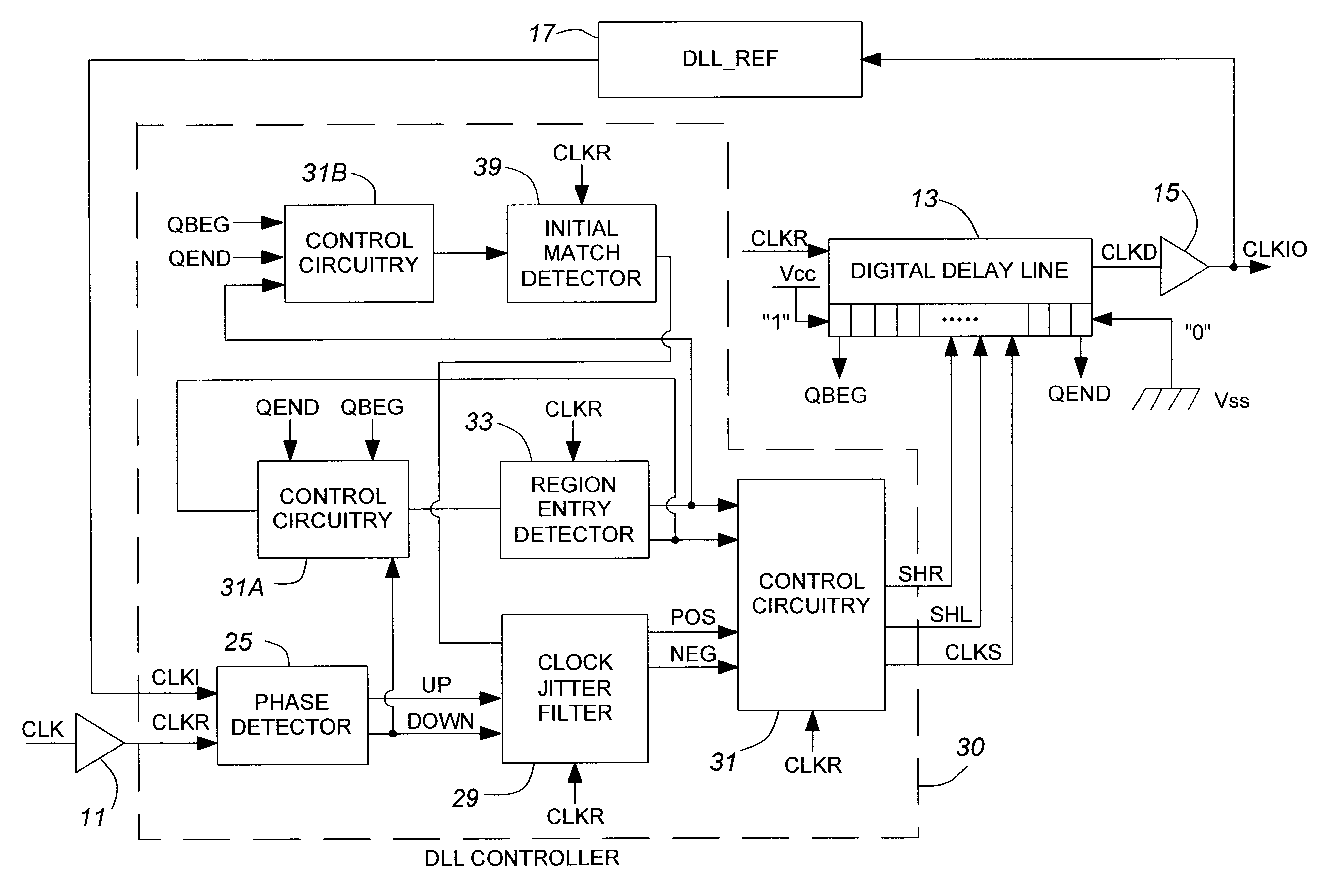
Figure 1 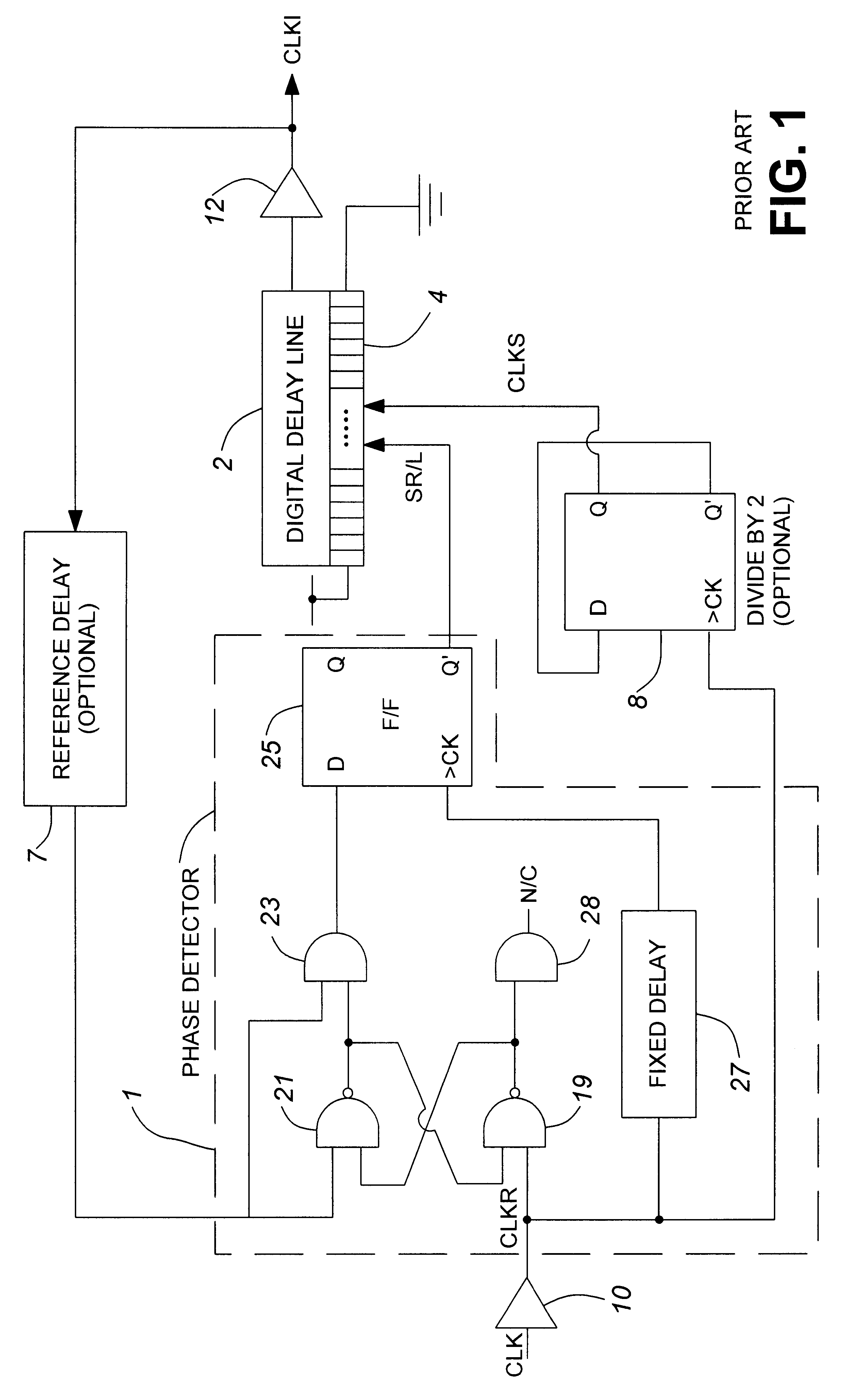
Figure 2 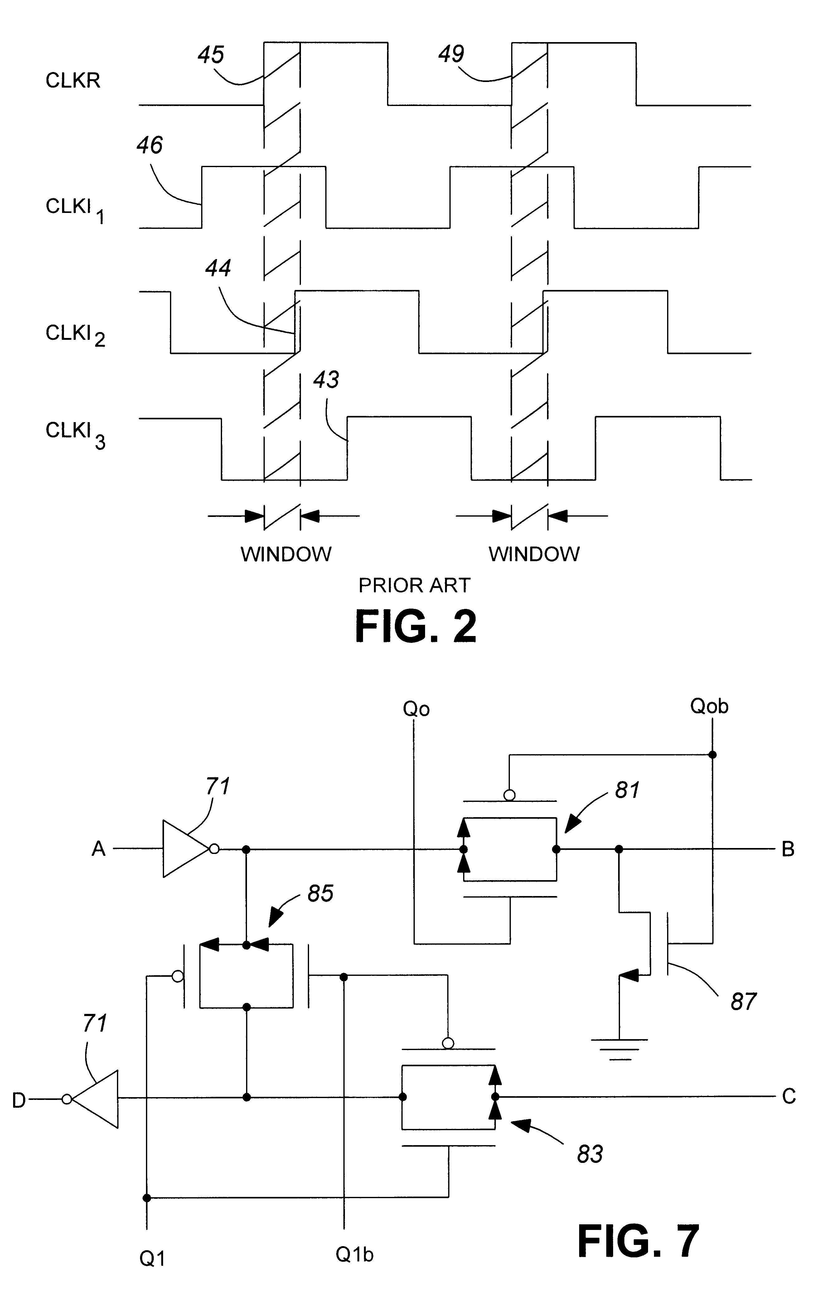
Figure 3
Abstract
Description
This invention relates to digital delay locked loops for use in high frequency clock synchronization applications.BACKGROUND TO THE INVENTIONIn synchronous dynamic random access memory (SDRAM) applications, as frequencies approach 200 MHz, the inherent analog delay between an external, system or reference clock and the time output data is valid, is becoming a crucial constraint. Such a delay of e.g. 4-10 ns is large enough to make a following clock cycle overlap the data, i.e. the delay becomes large enough for data not to be ready at the output during one cycle, and it essentially becomes "off-sync". This inherent internal delay must therefore be accelerated according to the necessary frequency but in a controlled fashion. The problem translates into a synchronization task between the internal clock, which controls the output path, and the correct edge of the external clock.Analog delay locked loops have been employed in the past to perform the synchronization, which are comprised ...
Examples
Embodiment Construction
FIG. 3 illustrates the main blocks used to form an embodiment of the present invention. An external main or system clock CLK is applied to a semiconductor device, passing through an input buffer 11 to become reference clock CLKR. Reference clock CLKR is fed from the output of the buffer to a phase detector 25. The outputs of the phase detector are coupled to control circuitry 31 via a clock jitter filter 29 (optional), as well as to other control circuitry 31A controlling a region entry detector 33. The region entry detector 33 inputs into control circuitry 31B to control both an initial phase match detector 39 as well as the shift left / right commands SHL, SHR. The digital delay line 13 receives the shift commands and produces the delayed clock signal CLKD, which in turn is buffered by a high fan-out clock driver 15 to a main internal input / output clock trunk line CLK_IO. The signal on the CLK_IO line is fed back through a reference delay circuit (DLL_REF) 17, to the phase detector ...