
Display device and a method of manufacturing the same
a technology of display device and manufacturing method, which is applied in the direction of solid-state device, electric lighting source, electric light source, etc., can solve the problems of shortest luminance life, relatively lower light emission efficiency of light emission device obtained by thermal transfer method described above, and relatively short luminance life compared with light emission device manufactured by shadow masking method, etc., to achieve good position accuracy, long luminance life of organic electroluminescent device, and high light emission efficiency
Patent Information
- Authority / Receiving Office
- US · United States
- Patent Type
- Patents(United States)
- Current Assignee / Owner
- Publication Date
- 2010-05-25
- Estimated Expiration
- Not applicable · inactive patent
Smart Images
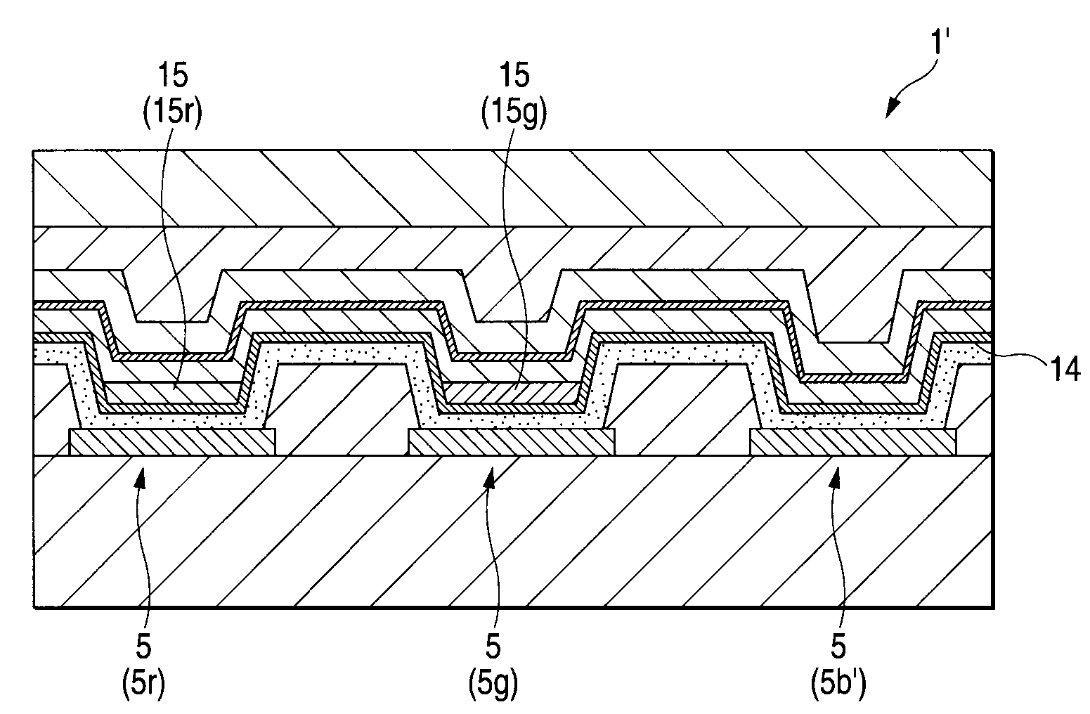
Figure 1 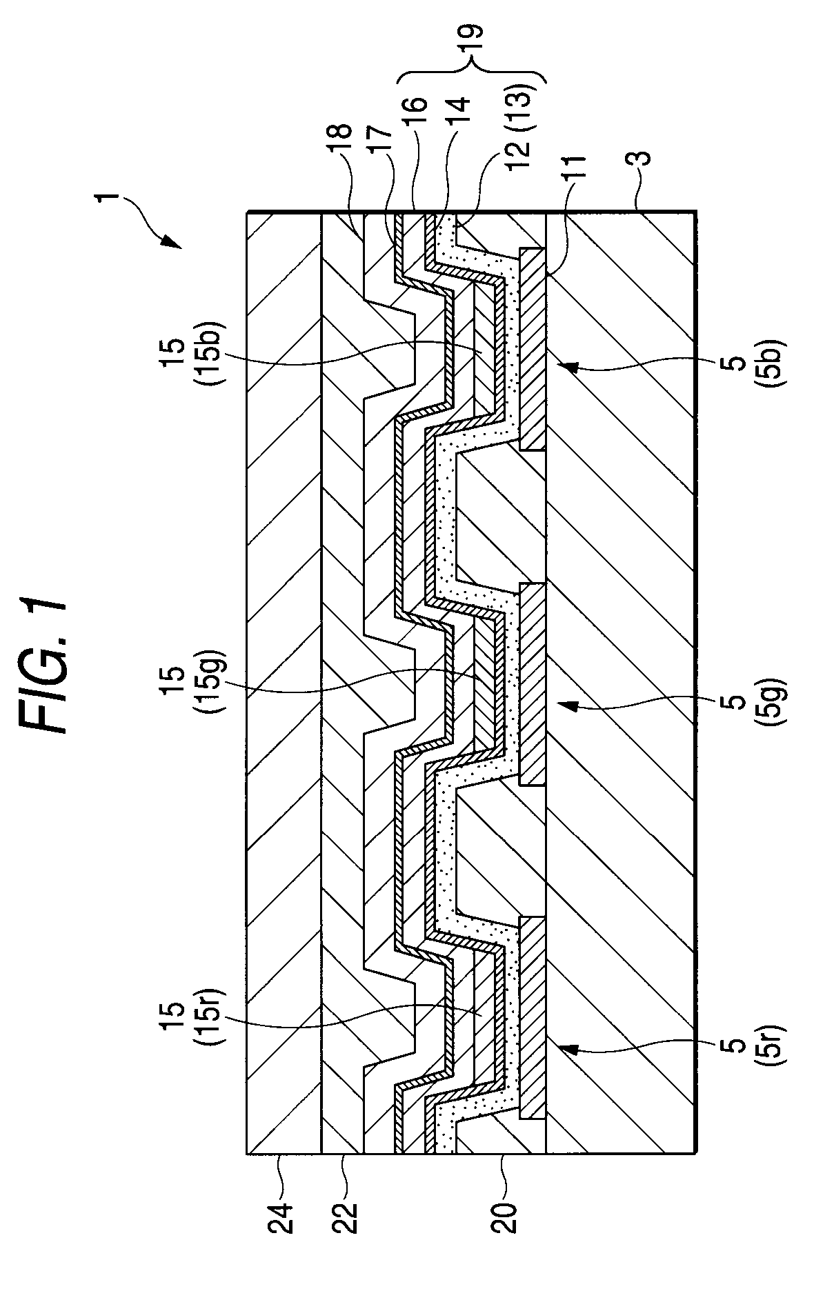
Figure 2 
Figure 3
Abstract
Description
CROSS REFERENCE TO RELATED APPLICATIONS
[0001] The present invention contains subject matter related to Japanese Patent Application JP 2005-119156 filed in the Japanese Patent Office on Apr. 18, 2005, the entire contents of which being incorporated herein by reference.BACKGROUND OF THE INVENTION
[0002] 1. Field of the Invention
[0003] The present invention concerns a display device and a manufacturing method thereof and, more specifically, it relates to a display device capable of color display using an organic electroluminescence device and a manufacturing method thereof.
[0004] 2. Description of the Related Art
[0005] In organic electroluminescence devices, organic layers such as a hole transporting layer and a light emitting layer are provided between a lower electrode and an upper electrode.
[0006] In full color display devices using the organic electroluminescence devices (hereinafter simply referred to as light emitting device), light emitting devices that emit respectively R (ref), G (gr...
Examples
first embodiment
[0018]FIG. 1 is a cross sectional view for main portion of a display device of a preferred embodiment as an example according to the invention. A display device 1 shown in the drawing is a flat panel display of full color indication in which a plurality of organic electroluminescence devices 5 (5r, 5g, and 5b) that emit respectively red (R), green (G), or blue (B) light are arranged above a substrate 3. Hereinafter, an organic electroluminescence device 5 that emits a red light is referred to as a red light emitting device 5r, an organic electroluminescence device 5 that emits a green light is referred to as a green light emitting device 5b, and an organic electroluminescence device 5 that emits a blue light is referred as the blue light emitting device 5b.
[0019]In each of the organic electroluminescence devices 5 (5r, 5g, and 5b), patterned lower electrode 11, hole injecting layer 12, hole transporting layer 13, first light emitting layer 14, second light emitting layers 15 (15r, ...
second embodiment
[0074]FIG. 3 is a cross sectional view for a main portion of a display device as a second embodiment according to the invention. A display device 1′ in FIG. 3 is different from the display device 1 in FIG. 1 in that a blue light emitting device 5b′ has no second light emitting layer.
[0075]That is, a light emitting layer of a blue light emitting device 5b′ has only the first light emitting layer 14. In the display device 1, the first light emitting layer 14 emits light whose wavelength is equal to or shorter than that of blue light. In the display device 1′, the first light emitting layer 14 emits blue light.
[0076]Also in this embodiment, the first light emitting layer 14 formed by vapor deposition emits blue light efficiently. Therefore, the same effect as the first embodiment can be obtained.
[0077]In addition, according to the second embodiment, since thermal transfer steps are necessary only twice, the manufacturing process can be simplified.
[0078]This invention is applicable to t...
example 1
[0083]A red light emitting organic electroluminescence device 15r was prepared (refer to FIG. 1).[0084](1) At first, above a glass substrate as a device forming substrate, an APC (Ag—Pd—Cu) layer as a silver alloy layer (film thickness: 120 nm), and an ITO film as a transparent conductive layer (film thickness: 10 nm) were formed in this order to form a lower electrode 11 of a two-layered structure. Then, an insulating film 20 of silicon oxide was formed to a thickness of about 2 μm by a sputtering method in a state of covering the circumferential edge of the lower electrode 11. Then, the lower electrode 11 was exposed by lithography, on which m-MTDATA was vapor deposited at a film thickness of 25 nm as the hole injecting layer 12, and α-NPD was vapor deposited to a film thickness of 30 nm as the hole transporting layer 13.[0085](2) As the first light emitting layer 14, a host material AND mixed with 2.5% by weight of DPAVBi as a dopant material was vapor deposited to a film thickne...