

Advanced Reticle Inspection Algorithms for Bidirectional Image Mapping
MAY 20, 20268 MIN READ
Generate Your Research Report Instantly with AI Agent
Patsnap Eureka helps you evaluate technical feasibility & market potential.
Reticle Inspection Technology Background and Objectives
Reticle inspection technology has emerged as a critical component in semiconductor manufacturing, driven by the relentless pursuit of smaller feature sizes and higher device densities. As integrated circuits continue to scale down according to Moore's Law, the precision requirements for photolithography masks, commonly known as reticles, have reached unprecedented levels. These optical templates serve as the foundation for transferring circuit patterns onto silicon wafers, making their quality paramount to the success of the entire manufacturing process.
The evolution of reticle inspection has been closely intertwined with advances in semiconductor node technology. Early inspection systems relied on simple optical comparison methods, but as feature sizes approached the wavelength of inspection light, traditional approaches became insufficient. The introduction of extreme ultraviolet (EUV) lithography and the transition to sub-10nm technology nodes have further intensified the challenges, demanding inspection capabilities that can detect defects smaller than 20 nanometers with high accuracy and throughput.
Bidirectional image mapping represents a significant advancement in reticle inspection methodology. This approach leverages the principle of capturing and analyzing images from multiple angles and orientations, enabling more comprehensive defect detection and characterization. Unlike conventional single-direction inspection systems, bidirectional mapping provides enhanced sensitivity to various defect types, including phase defects, edge roughness, and critical dimension variations that could significantly impact final device performance.
The primary objective of advanced reticle inspection algorithms for bidirectional image mapping is to achieve defect detection sensitivity below 15 nanometers while maintaining inspection throughput suitable for high-volume manufacturing environments. This requires sophisticated image processing algorithms capable of handling the complex optical interactions between inspection light and nanoscale features on the reticle surface.
Current technological goals focus on developing algorithms that can effectively correlate bidirectional image data to identify subtle pattern deviations, phase errors, and contamination particles. The integration of machine learning and artificial intelligence techniques has become increasingly important, enabling adaptive inspection strategies that can learn from historical defect patterns and optimize detection parameters in real-time.
The ultimate aim is to establish a robust inspection framework that not only detects existing defects but also predicts potential failure modes, thereby supporting proactive quality control measures in advanced semiconductor manufacturing processes.
The evolution of reticle inspection has been closely intertwined with advances in semiconductor node technology. Early inspection systems relied on simple optical comparison methods, but as feature sizes approached the wavelength of inspection light, traditional approaches became insufficient. The introduction of extreme ultraviolet (EUV) lithography and the transition to sub-10nm technology nodes have further intensified the challenges, demanding inspection capabilities that can detect defects smaller than 20 nanometers with high accuracy and throughput.
Bidirectional image mapping represents a significant advancement in reticle inspection methodology. This approach leverages the principle of capturing and analyzing images from multiple angles and orientations, enabling more comprehensive defect detection and characterization. Unlike conventional single-direction inspection systems, bidirectional mapping provides enhanced sensitivity to various defect types, including phase defects, edge roughness, and critical dimension variations that could significantly impact final device performance.
The primary objective of advanced reticle inspection algorithms for bidirectional image mapping is to achieve defect detection sensitivity below 15 nanometers while maintaining inspection throughput suitable for high-volume manufacturing environments. This requires sophisticated image processing algorithms capable of handling the complex optical interactions between inspection light and nanoscale features on the reticle surface.
Current technological goals focus on developing algorithms that can effectively correlate bidirectional image data to identify subtle pattern deviations, phase errors, and contamination particles. The integration of machine learning and artificial intelligence techniques has become increasingly important, enabling adaptive inspection strategies that can learn from historical defect patterns and optimize detection parameters in real-time.
The ultimate aim is to establish a robust inspection framework that not only detects existing defects but also predicts potential failure modes, thereby supporting proactive quality control measures in advanced semiconductor manufacturing processes.
Market Demand for Advanced Reticle Inspection Solutions
The semiconductor manufacturing industry faces unprecedented challenges in maintaining yield rates and product quality as device geometries continue to shrink below 5nm nodes. Advanced reticle inspection has emerged as a critical bottleneck in the production workflow, with traditional inspection methods struggling to detect increasingly subtle defects that can cause catastrophic yield losses. The demand for sophisticated inspection algorithms capable of bidirectional image mapping has intensified as manufacturers seek to identify and classify defects with higher precision and speed.
Foundries and integrated device manufacturers are experiencing significant pressure to reduce inspection cycle times while simultaneously improving defect detection sensitivity. Current inspection processes often require multiple passes and extensive manual review, creating production bottlenecks that directly impact time-to-market for critical semiconductor products. The industry requires inspection solutions that can process complex reticle patterns in both forward and reverse mapping configurations to ensure comprehensive defect coverage.
The proliferation of extreme ultraviolet lithography and advanced packaging technologies has created new inspection challenges that existing solutions cannot adequately address. Multi-patterning techniques and complex optical proximity correction features demand inspection algorithms capable of understanding bidirectional relationships between design intent and manufactured patterns. This technological evolution has generated substantial market pull for next-generation inspection capabilities.
Leading semiconductor manufacturers are actively seeking inspection solutions that can integrate seamlessly with existing manufacturing execution systems while providing real-time feedback for process optimization. The ability to perform bidirectional image mapping enables more accurate defect classification and reduces false positive rates, which currently consume significant engineering resources in manual review processes.
Market drivers include the increasing cost of mask sets, which can exceed several million dollars for advanced nodes, making defect detection economics increasingly critical. Additionally, the growing complexity of photomask designs requires inspection algorithms that can adapt to diverse pattern types and geometries while maintaining consistent performance across different reticle technologies.
The demand extends beyond traditional logic and memory manufacturers to include emerging applications in automotive semiconductors, artificial intelligence chips, and advanced packaging solutions, where reliability requirements are driving more stringent inspection standards and creating new market opportunities for advanced algorithmic approaches.
Foundries and integrated device manufacturers are experiencing significant pressure to reduce inspection cycle times while simultaneously improving defect detection sensitivity. Current inspection processes often require multiple passes and extensive manual review, creating production bottlenecks that directly impact time-to-market for critical semiconductor products. The industry requires inspection solutions that can process complex reticle patterns in both forward and reverse mapping configurations to ensure comprehensive defect coverage.
The proliferation of extreme ultraviolet lithography and advanced packaging technologies has created new inspection challenges that existing solutions cannot adequately address. Multi-patterning techniques and complex optical proximity correction features demand inspection algorithms capable of understanding bidirectional relationships between design intent and manufactured patterns. This technological evolution has generated substantial market pull for next-generation inspection capabilities.
Leading semiconductor manufacturers are actively seeking inspection solutions that can integrate seamlessly with existing manufacturing execution systems while providing real-time feedback for process optimization. The ability to perform bidirectional image mapping enables more accurate defect classification and reduces false positive rates, which currently consume significant engineering resources in manual review processes.
Market drivers include the increasing cost of mask sets, which can exceed several million dollars for advanced nodes, making defect detection economics increasingly critical. Additionally, the growing complexity of photomask designs requires inspection algorithms that can adapt to diverse pattern types and geometries while maintaining consistent performance across different reticle technologies.
The demand extends beyond traditional logic and memory manufacturers to include emerging applications in automotive semiconductors, artificial intelligence chips, and advanced packaging solutions, where reliability requirements are driving more stringent inspection standards and creating new market opportunities for advanced algorithmic approaches.
Current State of Bidirectional Image Mapping Challenges
Bidirectional image mapping in advanced reticle inspection faces significant computational complexity challenges that limit real-time processing capabilities. Current algorithms struggle with the intensive mathematical operations required to establish accurate correspondence between reference and inspection images, particularly when dealing with high-resolution photomasks containing billions of features. The computational burden increases exponentially with image resolution and pattern density, creating bottlenecks in manufacturing throughput.
Registration accuracy remains a critical challenge in existing bidirectional mapping systems. Traditional feature-based registration methods often fail when confronted with repetitive semiconductor patterns, leading to false correspondences and misalignment errors. The sub-nanometer precision requirements of advanced lithography nodes demand registration accuracy that exceeds the capabilities of conventional correlation-based algorithms, particularly in the presence of systematic distortions and local pattern variations.
Noise interference and signal degradation present substantial obstacles in current mapping implementations. Optical inspection systems generate images with varying noise characteristics depending on illumination conditions, detector sensitivity, and environmental factors. Existing algorithms lack robust noise filtering mechanisms that can preserve critical defect information while eliminating spurious signals that corrupt the bidirectional mapping process.
Pattern complexity in modern semiconductor designs introduces unprecedented challenges for mapping algorithms. Advanced technology nodes feature intricate layouts with multiple patterning techniques, creating overlapping structures and complex geometries that confuse traditional mapping approaches. Current solutions struggle to maintain mapping fidelity across diverse pattern types, from dense memory arrays to irregular logic circuits, resulting in inconsistent inspection performance.
Real-time processing constraints impose severe limitations on current bidirectional mapping implementations. Manufacturing environments require inspection speeds that often exceed the processing capabilities of existing algorithms, forcing compromises between mapping accuracy and throughput. The lack of efficient parallel processing architectures and optimized computational frameworks prevents current systems from achieving the performance levels demanded by high-volume semiconductor production.
Scalability issues plague existing mapping solutions as they attempt to handle increasingly larger die sizes and more complex mask layouts. Current algorithms exhibit poor scaling characteristics, with processing times growing disproportionately as pattern complexity increases, limiting their applicability to next-generation semiconductor technologies.
Registration accuracy remains a critical challenge in existing bidirectional mapping systems. Traditional feature-based registration methods often fail when confronted with repetitive semiconductor patterns, leading to false correspondences and misalignment errors. The sub-nanometer precision requirements of advanced lithography nodes demand registration accuracy that exceeds the capabilities of conventional correlation-based algorithms, particularly in the presence of systematic distortions and local pattern variations.
Noise interference and signal degradation present substantial obstacles in current mapping implementations. Optical inspection systems generate images with varying noise characteristics depending on illumination conditions, detector sensitivity, and environmental factors. Existing algorithms lack robust noise filtering mechanisms that can preserve critical defect information while eliminating spurious signals that corrupt the bidirectional mapping process.
Pattern complexity in modern semiconductor designs introduces unprecedented challenges for mapping algorithms. Advanced technology nodes feature intricate layouts with multiple patterning techniques, creating overlapping structures and complex geometries that confuse traditional mapping approaches. Current solutions struggle to maintain mapping fidelity across diverse pattern types, from dense memory arrays to irregular logic circuits, resulting in inconsistent inspection performance.
Real-time processing constraints impose severe limitations on current bidirectional mapping implementations. Manufacturing environments require inspection speeds that often exceed the processing capabilities of existing algorithms, forcing compromises between mapping accuracy and throughput. The lack of efficient parallel processing architectures and optimized computational frameworks prevents current systems from achieving the performance levels demanded by high-volume semiconductor production.
Scalability issues plague existing mapping solutions as they attempt to handle increasingly larger die sizes and more complex mask layouts. Current algorithms exhibit poor scaling characteristics, with processing times growing disproportionately as pattern complexity increases, limiting their applicability to next-generation semiconductor technologies.
Existing Bidirectional Image Mapping Solutions
01 Image alignment and registration techniques for reticle inspection
Advanced algorithms for precise alignment and registration of reticle images during inspection processes. These techniques ensure accurate positioning and correlation between reference images and captured inspection data, enabling reliable defect detection through proper image mapping and geometric transformation methods.- Image alignment and registration techniques for reticle inspection: Advanced algorithms for precise alignment and registration of reticle images during inspection processes. These techniques ensure accurate positioning and correlation between reference images and captured inspection data, enabling reliable defect detection through proper image mapping and geometric transformation methods.
- Pattern matching and template-based inspection algorithms: Sophisticated pattern recognition systems that utilize template matching and correlation algorithms to identify defects in reticle structures. These methods compare captured images against reference patterns to detect deviations, anomalies, and manufacturing defects through advanced computational analysis and feature extraction techniques.
- Machine learning and AI-based defect classification systems: Intelligent inspection systems that employ machine learning algorithms and artificial intelligence for automated defect detection and classification. These advanced systems can learn from inspection data to improve accuracy over time and provide sophisticated analysis of complex reticle patterns and potential manufacturing issues.
- Multi-scale and hierarchical image processing methods: Comprehensive inspection approaches that analyze reticle images at multiple resolution levels and scales. These hierarchical methods enable efficient processing of large-scale reticle data while maintaining sensitivity to fine details, optimizing both inspection speed and detection accuracy through adaptive sampling and processing strategies.
- Real-time inspection and parallel processing architectures: High-performance computing systems designed for real-time reticle inspection with parallel processing capabilities. These architectures enable rapid image analysis and mapping through distributed computing methods, optimized data flow management, and specialized hardware implementations for industrial manufacturing environments.
02 Pattern matching and template-based inspection algorithms
Sophisticated pattern recognition methods that utilize template matching for identifying defects and anomalies in reticle structures. These algorithms compare captured images against reference patterns to detect deviations, utilizing correlation techniques and feature extraction to ensure high-accuracy inspection results.Expand Specific Solutions03 Machine learning and AI-based defect classification systems
Implementation of artificial intelligence and machine learning algorithms for automated defect detection and classification in reticle inspection. These systems utilize neural networks and deep learning approaches to improve inspection accuracy and reduce false positive rates through intelligent image analysis.Expand Specific Solutions04 Multi-scale and hierarchical image processing methods
Advanced image processing techniques that analyze reticle patterns at multiple resolution levels and scales. These methods employ hierarchical approaches to efficiently process large-scale reticle images while maintaining sensitivity to small defects through pyramid-based algorithms and multi-resolution analysis.Expand Specific Solutions05 Real-time image enhancement and noise reduction algorithms
Signal processing techniques designed to improve image quality and reduce noise in reticle inspection systems. These algorithms enhance contrast, reduce artifacts, and optimize image characteristics for better defect visibility while maintaining processing speed requirements for industrial applications.Expand Specific Solutions
Key Players in Reticle Inspection Equipment Industry
The advanced reticle inspection algorithms for bidirectional image mapping field represents a mature technology sector within the semiconductor manufacturing ecosystem, currently experiencing steady growth driven by increasing demand for precision lithography processes. The market demonstrates significant scale, supported by established players across multiple segments including semiconductor equipment manufacturers like Mitsubishi Electric Corp., Siemens AG, and Mycronic AB, research institutions such as CEA and University of Surrey, and specialized technology companies like Nexchip Semiconductor Corp. and ImmerVision Inc. Technology maturity varies across applications, with traditional inspection methods well-established while AI-enhanced bidirectional mapping algorithms represent emerging capabilities. The competitive landscape shows consolidation around major industrial conglomerates alongside specialized niche players, indicating both market stability and ongoing innovation opportunities in advanced imaging and defect detection methodologies.
Mitsubishi Electric Corp.
Technical Solution: Mitsubishi Electric has developed comprehensive reticle inspection solutions featuring advanced optical and electron beam inspection technologies. Their bidirectional image mapping algorithms incorporate deep learning neural networks to analyze pattern fidelity and detect critical dimension variations across photomasks. The system performs simultaneous forward and backward image correlation to identify defects that could impact lithographic printing quality. Their technology supports inspection of EUV masks and advanced ArF immersion masks, with capability to detect defects down to 15nm while processing inspection data at rates exceeding 500 GB/hour. The algorithms include automated defect classification and disposition recommendations based on printability impact analysis.
Strengths: Comprehensive inspection coverage for multiple mask types, strong integration with manufacturing workflows. Weaknesses: Limited to certain semiconductor technology nodes, requires significant computational resources.
Siemens AG
Technical Solution: Siemens has developed industrial imaging and inspection solutions that incorporate bidirectional mapping algorithms for quality control applications. Their technology utilizes advanced computer vision algorithms with machine learning capabilities to perform automated defect detection and pattern analysis. The system employs multi-directional image acquisition and processing techniques to create comprehensive inspection maps of manufactured components. Their algorithms can process high-resolution images in real-time, detecting anomalies and variations in manufactured patterns with sub-micron precision. The bidirectional mapping approach enables correlation between design intent and actual manufactured results, supporting quality assurance in precision manufacturing environments including semiconductor and automotive applications.
Strengths: Robust industrial automation integration, scalable across multiple manufacturing sectors. Weaknesses: Less specialized for semiconductor reticle inspection compared to dedicated mask inspection vendors.
Core Algorithm Innovations in Reticle Inspection
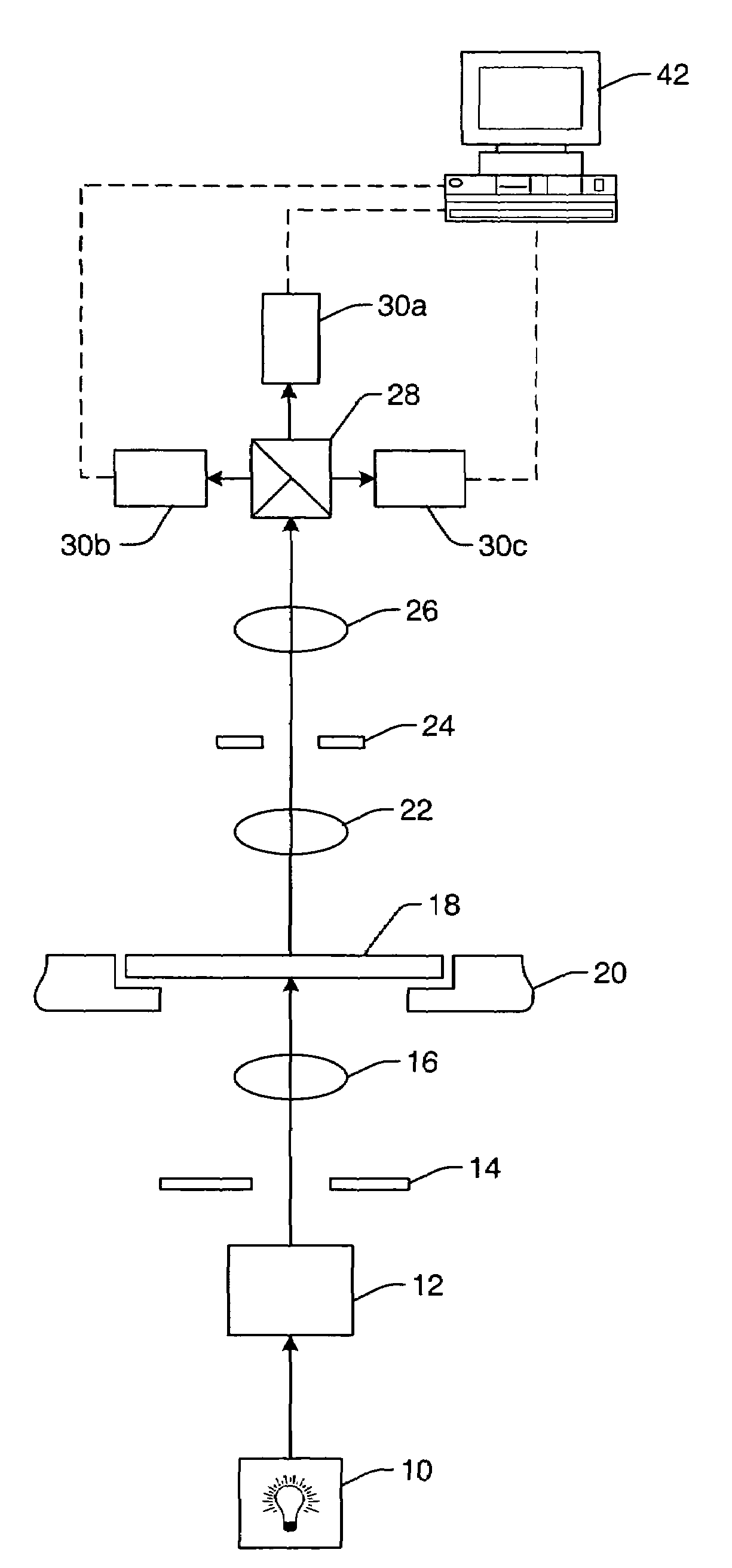
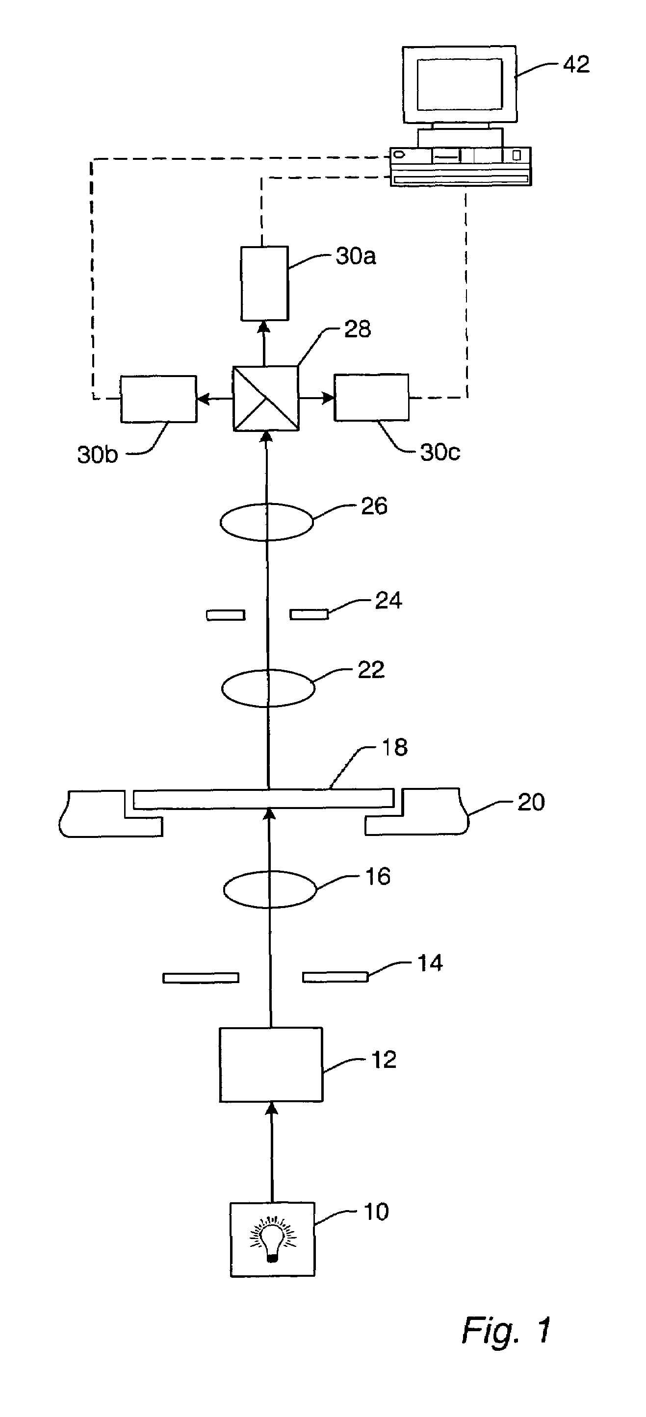
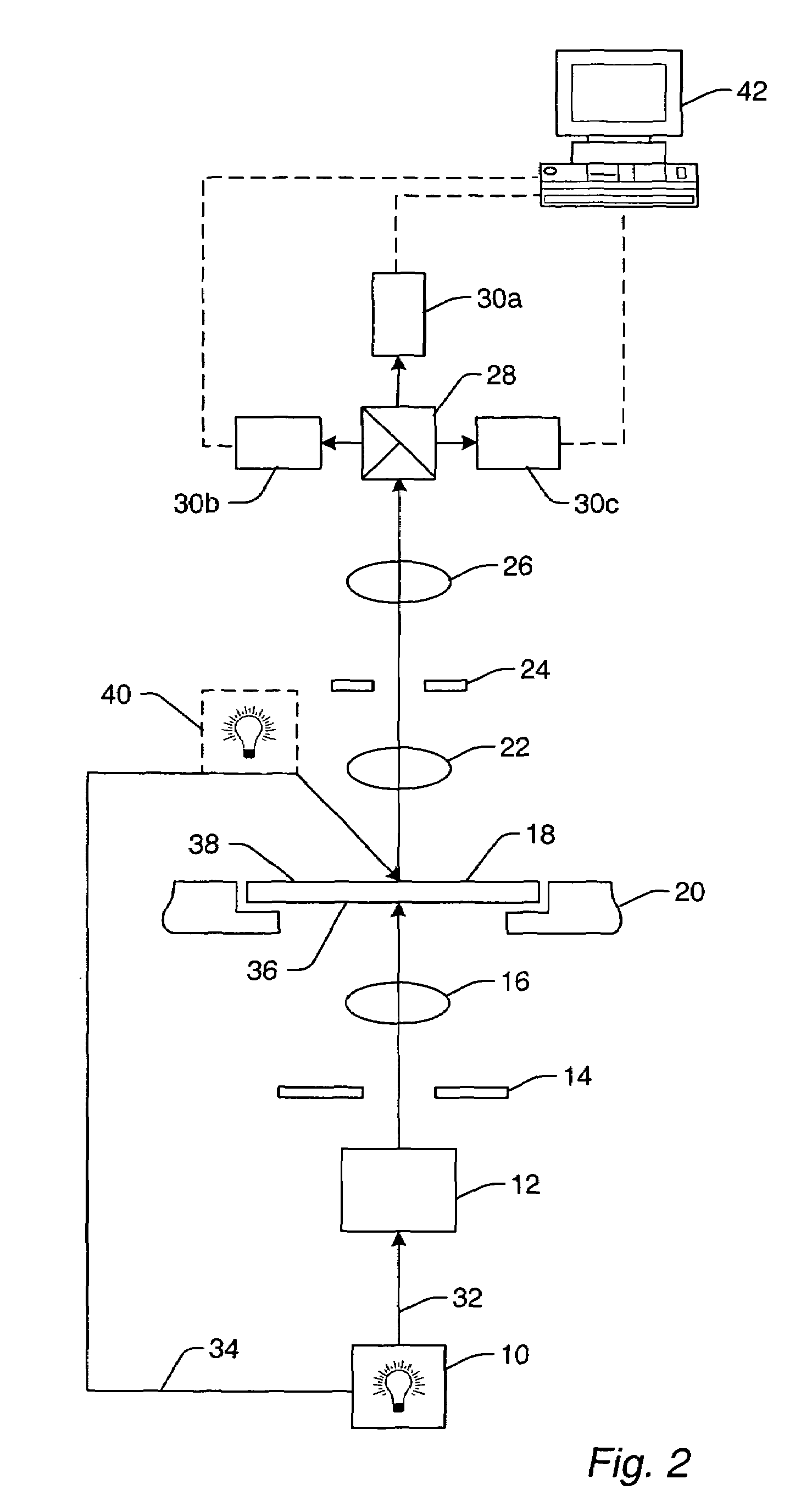
Apparatus and methods for inspecting reticles
PatentActiveUS20180082415A1
Innovation
- A method and system for qualifying photolithographic reticles by acquiring images at different illumination and imaging configurations to recover the reticle near field, which is then analyzed to determine potential wafer pattern defects and stability, using a lithography model to simulate wafer images and compare them under various process conditions.


Methods and systems for reticle inspection and defect review using aerial imaging
PatentInactiveUS7379175B1
Innovation
- A method and system for inspecting reticles using aerial imaging, where a set of exposure conditions forms an aerial image of the reticle, and defects are detected by comparing this image to a reference image stored in a database, excluding optical proximity correction features, allowing for the identification of defects that would be printed onto a specimen.

Semiconductor Manufacturing Quality Standards
Semiconductor manufacturing quality standards for advanced reticle inspection represent a critical framework governing the precision and reliability requirements in photolithography processes. These standards establish the foundational metrics that determine acceptable defect densities, pattern fidelity tolerances, and inspection sensitivity thresholds essential for maintaining yield optimization in semiconductor fabrication facilities.
The International Technology Roadmap for Semiconductors (ITRS) and subsequent IEEE standards define stringent specifications for reticle quality control, particularly emphasizing defect detection capabilities below 20 nanometers for advanced technology nodes. These standards mandate comprehensive inspection protocols that encompass both programmed defects and random particle contamination, requiring detection sensitivities that can identify critical dimension variations within 2-3% tolerance ranges.
Quality assurance frameworks specifically address bidirectional image mapping accuracy, establishing requirements for geometric distortion correction within sub-nanometer precision levels. The standards stipulate that inspection algorithms must demonstrate consistent performance across varying illumination conditions, pattern densities, and substrate materials while maintaining false positive rates below 0.1% to ensure manufacturing efficiency.
Metrology standards integrate statistical process control methodologies, requiring real-time monitoring of inspection system performance through standardized test reticles and reference artifacts. These protocols ensure that advanced inspection algorithms maintain calibration accuracy throughout extended operational periods, with mandatory recertification cycles aligned with semiconductor manufacturing quality management systems.
Compliance verification procedures encompass both hardware and software validation, mandating that bidirectional image mapping algorithms undergo rigorous qualification testing against industry-standard defect libraries. The standards require comprehensive documentation of algorithm performance characteristics, including sensitivity curves, throughput metrics, and correlation studies with alternative inspection methodologies to establish traceability and reproducibility in quality assessment processes.
The International Technology Roadmap for Semiconductors (ITRS) and subsequent IEEE standards define stringent specifications for reticle quality control, particularly emphasizing defect detection capabilities below 20 nanometers for advanced technology nodes. These standards mandate comprehensive inspection protocols that encompass both programmed defects and random particle contamination, requiring detection sensitivities that can identify critical dimension variations within 2-3% tolerance ranges.
Quality assurance frameworks specifically address bidirectional image mapping accuracy, establishing requirements for geometric distortion correction within sub-nanometer precision levels. The standards stipulate that inspection algorithms must demonstrate consistent performance across varying illumination conditions, pattern densities, and substrate materials while maintaining false positive rates below 0.1% to ensure manufacturing efficiency.
Metrology standards integrate statistical process control methodologies, requiring real-time monitoring of inspection system performance through standardized test reticles and reference artifacts. These protocols ensure that advanced inspection algorithms maintain calibration accuracy throughout extended operational periods, with mandatory recertification cycles aligned with semiconductor manufacturing quality management systems.
Compliance verification procedures encompass both hardware and software validation, mandating that bidirectional image mapping algorithms undergo rigorous qualification testing against industry-standard defect libraries. The standards require comprehensive documentation of algorithm performance characteristics, including sensitivity curves, throughput metrics, and correlation studies with alternative inspection methodologies to establish traceability and reproducibility in quality assessment processes.
Cost-Benefit Analysis of Advanced Inspection Systems
The implementation of advanced reticle inspection systems utilizing bidirectional image mapping algorithms requires substantial capital investment, yet delivers significant long-term value through enhanced defect detection capabilities and reduced manufacturing risks. Initial system acquisition costs typically range from $15-25 million per unit, with additional expenses for facility modifications, specialized training programs, and integration with existing manufacturing execution systems.
Operational expenditures encompass algorithm maintenance, software licensing, computational infrastructure upgrades, and skilled personnel requirements. Advanced bidirectional mapping algorithms demand high-performance computing resources, contributing approximately 20-30% to total operational costs. However, these systems demonstrate superior throughput compared to conventional inspection methods, processing reticles 40-60% faster while maintaining higher accuracy standards.
The primary financial benefits emerge through defect escape reduction and yield improvement. Advanced algorithms can detect critical defects with 95-98% accuracy, compared to 85-90% for traditional systems. This enhanced detection capability translates to substantial cost avoidance, as a single escaped defect can result in $2-5 million in downstream manufacturing losses and customer returns.
Return on investment calculations indicate break-even points typically occurring within 18-24 months for high-volume manufacturing facilities. The bidirectional mapping capability enables comprehensive defect characterization, reducing false positive rates by 35-45% and minimizing unnecessary reticle rework cycles. This efficiency improvement generates additional cost savings through reduced material waste and shortened production cycles.
Risk mitigation represents another significant benefit dimension. Advanced inspection systems provide enhanced process control visibility, enabling proactive quality management and reducing the probability of catastrophic yield events. Insurance and liability cost reductions, combined with improved customer satisfaction metrics, contribute to the overall value proposition of these sophisticated inspection technologies.
Operational expenditures encompass algorithm maintenance, software licensing, computational infrastructure upgrades, and skilled personnel requirements. Advanced bidirectional mapping algorithms demand high-performance computing resources, contributing approximately 20-30% to total operational costs. However, these systems demonstrate superior throughput compared to conventional inspection methods, processing reticles 40-60% faster while maintaining higher accuracy standards.
The primary financial benefits emerge through defect escape reduction and yield improvement. Advanced algorithms can detect critical defects with 95-98% accuracy, compared to 85-90% for traditional systems. This enhanced detection capability translates to substantial cost avoidance, as a single escaped defect can result in $2-5 million in downstream manufacturing losses and customer returns.
Return on investment calculations indicate break-even points typically occurring within 18-24 months for high-volume manufacturing facilities. The bidirectional mapping capability enables comprehensive defect characterization, reducing false positive rates by 35-45% and minimizing unnecessary reticle rework cycles. This efficiency improvement generates additional cost savings through reduced material waste and shortened production cycles.
Risk mitigation represents another significant benefit dimension. Advanced inspection systems provide enhanced process control visibility, enabling proactive quality management and reducing the probability of catastrophic yield events. Insurance and liability cost reductions, combined with improved customer satisfaction metrics, contribute to the overall value proposition of these sophisticated inspection technologies.
Unlock deeper insights with Patsnap Eureka Quick Research — get a full tech report to explore trends and direct your research. Try now!
Generate Your Research Report Instantly with AI Agent
Supercharge your innovation with Patsnap Eureka AI Agent Platform!